SI840XI2C-KIT Silicon Laboratories Inc, SI840XI2C-KIT Datasheet - Page 6
SI840XI2C-KIT
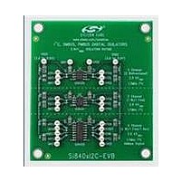
Manufacturer Part Number
SI840XI2C-KIT
Description
KIT EVAL FOR SI840X
Manufacturer
Silicon Laboratories Inc
Specifications of SI840XI2C-KIT
Main Purpose
Interface, Digital Isolator
Embedded
No
Utilized Ic / Part
Si8400, Si8401, Si8405
Primary Attributes
Assorted Bi-directional i²C Isolators
Secondary Attributes
2 Single Channel, 1 Dual channel isolator
Interface Type
I2C
Operating Supply Voltage
2.7 V to 5.5 V
Product
Interface Modules
For Use With/related Products
Si840x
Lead Free Status / RoHS Status
Lead free / RoHS Compliant
Lead Free Status / RoHS Status
Lead free / RoHS Compliant, Lead free / RoHS Compliant
Other names
336-1990


Si840x
Table 3. Si8400/01/02/05 Electrical Characteristics for Bidirectional I
3.0 V < VDD < 5.5 V. TA = –40 to +125 °C. Typical specs at 25 °C unless otherwise noted.
6
Timing Specifications (Measured at 1.40 V Unless Otherwise Specified)
Maximum I
Propagation Delay
5 V Operation
Side A to side B rising
Side A to side B falling
Side B to side A rising
Side B to side A falling
3.3 V Operation
Side A to side B rising
Side A to side B falling
Side B to side A rising
Side B to side A falling
Pulse width distortion
5 V
Side A low to Side B low
Side B low to Side A low
3.3 V
Side A low to Side B low
Side B low to Side A low
Notes:
1. All voltages are relative to respective ground.
2. V
3. Logic low output voltages are 910 mV max from –10 to 125 °C at 3.0 mA.
4. I
5. Side A measured at 0.6 V.
Logic low output voltages are 955 mV max from –40 to 125 °C at 3.0 mA.
Logic low output voltages are 825 mV max from –10 to 125 °C at 0.5 mA.
Logic low output voltages are 875 mV max from –40 to 125 °C at 0.5 mA.
See “AN375: Design Considerations for Isolating an I
minimum difference between the output logic low level of the driving device and the input logic threshold.
2
IL
CV (Side A) = I
< 0.450 V, V
Parameter
2
C bus Frequency
IH
5
5
5
5
2
> 0.780 V.
CV
5
5
OL
(Side A) – I
Symbol
PWDAB
PWDBA
PWDAB
PWDBA
2
Tphab
Tphba
Tphab
Tphba
Fmax
Tplab
Tplba
Tplab
Tplba
CV
T
(Side A). To ensure no latch-up on a given bus, I
Rev. 1.3
2
C Bus or SMBus” for additional information.
No bus capacitance,
No bus capacitance,
Test Condition
See Figure 2
See Figure 2
R1 = 1400,
R1 = 1400,
R2 = 499,
R2 = 499,
R1 = 806,
R1 = 806
R2 = 499
R2 = 499
2
C Channels
Min
—
—
—
—
—
—
—
—
—
—
—
—
—
2
CV (Side A) is the
Typ
9.0
9.0
25
15
20
28
13
20
10
15
—
11
11
1
(Continued)
Max
1.7
29
22
30
12
35
18
40
15
15
20
22
30
Unit
MHz
ns
ns
ns
ns
ns
ns
ns
ns
ns
ns
ns
ns
Related parts for SI840XI2C-KIT
Image
Part Number
Description
Manufacturer
Datasheet
Request
R

Part Number:
Description:
SMD/C°/SINGLE-ENDED OUTPUT SILICON OSCILLATOR
Manufacturer:
Silicon Laboratories Inc
Part Number:
Description:
Manufacturer:
Silicon Laboratories Inc
Datasheet:
Part Number:
Description:
N/A N/A/SI4010 AES KEYFOB DEMO WITH LCD RX
Manufacturer:
Silicon Laboratories Inc
Datasheet:
Part Number:
Description:
N/A N/A/SI4010 SIMPLIFIED KEY FOB DEMO WITH LED RX
Manufacturer:
Silicon Laboratories Inc
Datasheet:
Part Number:
Description:
N/A/-40 TO 85 OC/EZLINK MODULE; F930/4432 HIGH BAND (REV E/B1)
Manufacturer:
Silicon Laboratories Inc
Part Number:
Description:
EZLink Module; F930/4432 Low Band (rev e/B1)
Manufacturer:
Silicon Laboratories Inc
Part Number:
Description:
I°/4460 10 DBM RADIO TEST CARD 434 MHZ
Manufacturer:
Silicon Laboratories Inc
Part Number:
Description:
I°/4461 14 DBM RADIO TEST CARD 868 MHZ
Manufacturer:
Silicon Laboratories Inc
Part Number:
Description:
I°/4463 20 DBM RFSWITCH RADIO TEST CARD 460 MHZ
Manufacturer:
Silicon Laboratories Inc
Part Number:
Description:
I°/4463 20 DBM RADIO TEST CARD 868 MHZ
Manufacturer:
Silicon Laboratories Inc
Part Number:
Description:
I°/4463 27 DBM RADIO TEST CARD 868 MHZ
Manufacturer:
Silicon Laboratories Inc
Part Number:
Description:
I°/4463 SKYWORKS 30 DBM RADIO TEST CARD 915 MHZ
Manufacturer:
Silicon Laboratories Inc
Part Number:
Description:
N/A N/A/-40 TO 85 OC/4463 RFMD 30 DBM RADIO TEST CARD 915 MHZ
Manufacturer:
Silicon Laboratories Inc
Part Number:
Description:
I°/4463 20 DBM RADIO TEST CARD 169 MHZ
Manufacturer:
Silicon Laboratories Inc