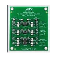
SI840XI2C-KIT Silicon Laboratories Inc, SI840XI2C-KIT Datasheet - Page 12
SI840XI2C-KIT
Manufacturer Part Number
SI840XI2C-KIT
Description
KIT EVAL FOR SI840X
Manufacturer
Silicon Laboratories Inc
Specifications of SI840XI2C-KIT
Main Purpose
Interface, Digital Isolator
Embedded
No
Utilized Ic / Part
Si8400, Si8401, Si8405
Primary Attributes
Assorted Bi-directional i²C Isolators
Secondary Attributes
2 Single Channel, 1 Dual channel isolator
Interface Type
I2C
Operating Supply Voltage
2.7 V to 5.5 V
Product
Interface Modules
For Use With/related Products
Si840x
Lead Free Status / RoHS Status
Lead free / RoHS Compliant
Lead Free Status / RoHS Status
Lead free / RoHS Compliant, Lead free / RoHS Compliant
Other names
336-1990


Si840x
2. Functional Description
2.1. Theory of Operation
The operation of an Si84xx channel is analogous to that of an opto coupler, except an RF carrier is modulated
instead of light. This simple architecture provides a robust isolated data path and requires no special
considerations or initialization at start-up. A simplified block diagram for a single unidirectional Si84xx channel is
shown in Figure 5.
A channel consists of an RF Transmitter and RF Receiver separated by a semiconductor-based isolation barrier.
Referring to the Transmitter, input A modulates the carrier provided by an RF oscillator using on/off keying. The
Receiver contains a demodulator that decodes the input state according to its RF energy content and applies the
result to output B via the output driver. This RF on/off keying scheme is superior to pulse code schemes as it
provides best-in-class noise immunity, low power consumption, and better immunity to magnetic fields. See
Figure 6 for more details.
12
A
Transmitter
OSCILLATOR
MODULATOR
Figure 5. Simplified Channel Diagram
RF
Figure 6. Modulation Scheme
Semiconductor-
Based Isolation
Rev. 1.3
Barrier
DEMODULATOR
Modulation Signal
Output Signal
Input Signal
Receiver
B
Related parts for SI840XI2C-KIT
Image
Part Number
Description
Manufacturer
Datasheet
Request
R

Part Number:
Description:
SMD/C°/SINGLE-ENDED OUTPUT SILICON OSCILLATOR
Manufacturer:
Silicon Laboratories Inc
Part Number:
Description:
Manufacturer:
Silicon Laboratories Inc
Datasheet:
Part Number:
Description:
N/A N/A/SI4010 AES KEYFOB DEMO WITH LCD RX
Manufacturer:
Silicon Laboratories Inc
Datasheet:
Part Number:
Description:
N/A N/A/SI4010 SIMPLIFIED KEY FOB DEMO WITH LED RX
Manufacturer:
Silicon Laboratories Inc
Datasheet:
Part Number:
Description:
N/A/-40 TO 85 OC/EZLINK MODULE; F930/4432 HIGH BAND (REV E/B1)
Manufacturer:
Silicon Laboratories Inc
Part Number:
Description:
EZLink Module; F930/4432 Low Band (rev e/B1)
Manufacturer:
Silicon Laboratories Inc
Part Number:
Description:
I°/4460 10 DBM RADIO TEST CARD 434 MHZ
Manufacturer:
Silicon Laboratories Inc
Part Number:
Description:
I°/4461 14 DBM RADIO TEST CARD 868 MHZ
Manufacturer:
Silicon Laboratories Inc
Part Number:
Description:
I°/4463 20 DBM RFSWITCH RADIO TEST CARD 460 MHZ
Manufacturer:
Silicon Laboratories Inc
Part Number:
Description:
I°/4463 20 DBM RADIO TEST CARD 868 MHZ
Manufacturer:
Silicon Laboratories Inc
Part Number:
Description:
I°/4463 27 DBM RADIO TEST CARD 868 MHZ
Manufacturer:
Silicon Laboratories Inc
Part Number:
Description:
I°/4463 SKYWORKS 30 DBM RADIO TEST CARD 915 MHZ
Manufacturer:
Silicon Laboratories Inc
Part Number:
Description:
N/A N/A/-40 TO 85 OC/4463 RFMD 30 DBM RADIO TEST CARD 915 MHZ
Manufacturer:
Silicon Laboratories Inc
Part Number:
Description:
I°/4463 20 DBM RADIO TEST CARD 169 MHZ
Manufacturer:
Silicon Laboratories Inc