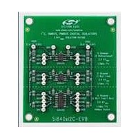
SI840XI2C-KIT Silicon Laboratories Inc, SI840XI2C-KIT Datasheet - Page 14
SI840XI2C-KIT
Manufacturer Part Number
SI840XI2C-KIT
Description
KIT EVAL FOR SI840X
Manufacturer
Silicon Laboratories Inc
Specifications of SI840XI2C-KIT
Main Purpose
Interface, Digital Isolator
Embedded
No
Utilized Ic / Part
Si8400, Si8401, Si8405
Primary Attributes
Assorted Bi-directional i²C Isolators
Secondary Attributes
2 Single Channel, 1 Dual channel isolator
Interface Type
I2C
Operating Supply Voltage
2.7 V to 5.5 V
Product
Interface Modules
For Use With/related Products
Si840x
Lead Free Status / RoHS Status
Lead free / RoHS Compliant
Lead Free Status / RoHS Status
Lead free / RoHS Compliant, Lead free / RoHS Compliant
Other names
336-1990


Si840x
3.3. Input and Output Characteristics for Non-I
The Si84xx inputs and outputs for unidirectional channels are standard CMOS drivers/receivers. The nominal
output impedance of an isolator driver channel is approximately 85 , ±40%, which is a combination of the value of
the on-chip series termination resistor and channel resistance of the output driver FET. When driving loads where
transmission line effects will be a factor, output pins should be appropriately terminated with controlled impedance
PCB traces. Table 12 details powered and unpowered operation of the Si84xx’s non-I
14
Notes:
V
I
1. VDDI and VDDO are the input and output power supplies. V
2. X = not applicable; H = Logic High; L = Logic Low.
3. Powered (P) state is defined as 3.0 V < VDD < 5.5 V.
4. Unpowered (UP) state is defined as VDD = 0 V.
5. Note that an I/O can power the die for a given side through an internal diode if its source has adequate current.
6. For I
Input
X
X
H
L
5
5
1,2
2
C channels, the outputs for a given side go to Hi-Z when power is lost on the opposite side.
VDDI State
UP
P
P
P
1,3,4
VDDO State
UP
P
P
P
Table 12. Si84xx Operation Table
1,3,4
Undetermined
V
O
Output
Rev. 1.3
L
H
L
6
1,2
2
I
C Digital Channels
and V
Normal operation.
Upon transition of VDDI from unpowered to pow-
ered, V
than 1 µs.
Upon transition of VDDO from unpowered to pow-
ered, V
1 µs.
O
are the respective input and output terminals.
O
O
returns to the same state as V
returns to the same state as V
Comments
2
C digital channels.
I
I
in less
within
Related parts for SI840XI2C-KIT
Image
Part Number
Description
Manufacturer
Datasheet
Request
R

Part Number:
Description:
SMD/C°/SINGLE-ENDED OUTPUT SILICON OSCILLATOR
Manufacturer:
Silicon Laboratories Inc
Part Number:
Description:
Manufacturer:
Silicon Laboratories Inc
Datasheet:
Part Number:
Description:
N/A N/A/SI4010 AES KEYFOB DEMO WITH LCD RX
Manufacturer:
Silicon Laboratories Inc
Datasheet:
Part Number:
Description:
N/A N/A/SI4010 SIMPLIFIED KEY FOB DEMO WITH LED RX
Manufacturer:
Silicon Laboratories Inc
Datasheet:
Part Number:
Description:
N/A/-40 TO 85 OC/EZLINK MODULE; F930/4432 HIGH BAND (REV E/B1)
Manufacturer:
Silicon Laboratories Inc
Part Number:
Description:
EZLink Module; F930/4432 Low Band (rev e/B1)
Manufacturer:
Silicon Laboratories Inc
Part Number:
Description:
I°/4460 10 DBM RADIO TEST CARD 434 MHZ
Manufacturer:
Silicon Laboratories Inc
Part Number:
Description:
I°/4461 14 DBM RADIO TEST CARD 868 MHZ
Manufacturer:
Silicon Laboratories Inc
Part Number:
Description:
I°/4463 20 DBM RFSWITCH RADIO TEST CARD 460 MHZ
Manufacturer:
Silicon Laboratories Inc
Part Number:
Description:
I°/4463 20 DBM RADIO TEST CARD 868 MHZ
Manufacturer:
Silicon Laboratories Inc
Part Number:
Description:
I°/4463 27 DBM RADIO TEST CARD 868 MHZ
Manufacturer:
Silicon Laboratories Inc
Part Number:
Description:
I°/4463 SKYWORKS 30 DBM RADIO TEST CARD 915 MHZ
Manufacturer:
Silicon Laboratories Inc
Part Number:
Description:
N/A N/A/-40 TO 85 OC/4463 RFMD 30 DBM RADIO TEST CARD 915 MHZ
Manufacturer:
Silicon Laboratories Inc
Part Number:
Description:
I°/4463 20 DBM RADIO TEST CARD 169 MHZ
Manufacturer:
Silicon Laboratories Inc