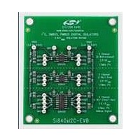
SI840XI2C-KIT Silicon Laboratories Inc, SI840XI2C-KIT Datasheet - Page 18

SI840XI2C-KIT
Manufacturer Part Number
SI840XI2C-KIT
Description
KIT EVAL FOR SI840X
Manufacturer
Silicon Laboratories Inc
Specifications of SI840XI2C-KIT
Main Purpose
Interface, Digital Isolator
Embedded
No
Utilized Ic / Part
Si8400, Si8401, Si8405
Primary Attributes
Assorted Bi-directional i²C Isolators
Secondary Attributes
2 Single Channel, 1 Dual channel isolator
Interface Type
I2C
Operating Supply Voltage
2.7 V to 5.5 V
Product
Interface Modules
For Use With/related Products
Si840x
Lead Free Status / RoHS Status
Lead free / RoHS Compliant
Lead Free Status / RoHS Status
Lead free / RoHS Compliant, Lead free / RoHS Compliant
Other names
336-1990
Si840x
5. Typical Application Overview
5.1. I
In many applications, I
elimination. For example, Power over Ethernet (PoE) applications typically use an I
between the PoE power sourcing device (PSE), and the earth ground referenced system controller. Galvanic
isolation is required both by standard and also as a practical matter to prevent ground loops in Ethernet connected
equipment.
The physical interface consists of two wires: serial data (SDA) and serial clock (SCL). These wires are connected
to open collector drivers that serve as both inputs and outputs. At first glance, it appears that SDA and SCL can be
isolated simply by placing two unidirectional isolators in parallel, and in opposite directions. However, this
technique creates feedback that latches the bus line low when a logic low asserted by either master or slave. This
problem can be remedied by adding anti-latch circuits, but results in a larger and more expensive solution. The
Si840x products offer a single-chip, anti-latch solution to the problem of isolating I
require no external components except the I
maximum of 2.5 kV
5.2. I
Without anti-latch protection, bidirectional I
through an adjacent isolator channel creating a stable latched low condition on both sides. Anti-latch protection is
typically added to one side of the isolator to avoid this condition (the “A” side for the Si8400/01/02/05).
The following examples illustrate typical circuit configurations using the Si8400/01/02/05.
The “A side” output low (V
isolator V
18
2
2
I2C/SMBus
C Background
C Isolator Operation
IL
Unit 1
to prevent the latch condition.
RMS
V
V
Figure 14. Isolated Bus Overview (Bidirectional Channels)
IL
, support I
2
OL
C, SMBus, and PMBus interfaces require galvanic isolation for safety or ground loop
OL
) and input low (V
2
C clock stretching, and operate to a maximum I
2
C isolators latch when an isolator output logic low propagates back
2
IL
C/SMBus pull-up resistors. In addition, they provide isolation to a
) levels are designed such that the isolator V
V
Si8400/01/02/05
OL
Rev. 1.3
V
ISO2
IL
+
-
ISO1
2
C bus speed of 1.7 Mbps.
2
C interface for communication
2
C/SMBus applications and
OL
is greater than the
I
2
C/SMBus
Unit 2


