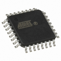
ATMEGA32M1-AU Atmel, ATMEGA32M1-AU Datasheet - Page 246

ATMEGA32M1-AU
Manufacturer Part Number
ATMEGA32M1-AU
Description
MPU AVR 32K FLASH 20MHZ 32TQFP
Manufacturer
Atmel
Series
AVR® ATmegar
Specifications of ATMEGA32M1-AU
Core Processor
AVR
Core Size
8-Bit
Speed
16MHz
Connectivity
CAN, LIN, SPI, UART/USART
Peripherals
Brown-out Detect/Reset, POR, PWM, Temp Sensor, WDT
Program Memory Size
32KB (16K x 16)
Program Memory Type
FLASH
Eeprom Size
1K x 8
Ram Size
2K x 8
Voltage - Supply (vcc/vdd)
2.7 V ~ 5.5 V
Data Converters
A/D 11x10b; D/A 1x10b
Oscillator Type
Internal
Operating Temperature
-40°C ~ 85°C
Package / Case
32-TQFP
Lead Free Status / RoHS Status
Lead free / RoHS Compliant
Number Of I /o
-
Available stocks
Company
Part Number
Manufacturer
Quantity
Price
Company:
Part Number:
ATMEGA32M1-AU
Manufacturer:
TYCO
Quantity:
210
- Current page: 246 of 341
- Download datasheet (6Mb)
21.10.5.1
21.10.5.2
21.10.6
21.10.7
246
ATmega16M1/32M1/64M1
DIDR0 – Digital Input Disable Register 0
DIDR1 – Digital Input Disable Register 1
ADLAR = 0
ADLAR = 1
Consequently, in 10-bit configuration, the ADCL register must be read first before the ADCH.
Nevertheless, to work easily with only 8-bit precision, there is the possibility to left adjust the
result thanks to the ADLAR bit in the ADCSRA register. Like this, it is sufficient to only read
ADCH to have the conversion result.
• Bit 7:0 – ADC7D..ADC0D, ACMPN0D, ACMPN1D, ACMPN2D, ACMPN3D, ACMP2D,
When this bit is written logic one, the digital input buffer on the corresponding ADC pin is dis-
abled. The corresponding PIN Register bit will always read as zero when this bit is set. When an
analog signal is applied to the ADC7:0 pin and the digital input from this pin is not needed, this
bit should be written logic one to reduce power consumption in the digital input buffer.
Bit
Read/Write
Initial Value
Bit
Read/Write
Initial Value
Bit
Read/Write
Initial Value
Bit
Read/Write
Initial Value
AMP2ND:
ADC7:0, ACMPN0, ACMPN1, ACMPN2, ACMPN3, ACMP2, AMP2N Digital Input Disable
ADC7D
ADC7
ADC9
ADC1
R/W
R
R
R
R
7
0
0
7
0
0
7
0
7
0
-
-
-
ACMPN1D
AMP2ND
AMP2PD
ADC6D
ADC6
ADC8
ADC0
R/W
6
0
6
0
R
R
R
R
6
0
0
6
0
0
-
-
ACMPN0D
ACMP0D
ADC5D
ADC5
ADC7
R/W
R/W
R
R
R
R
5
0
5
0
5
0
0
5
0
0
-
-
AMP0PD
ADC4D
ADC4
ADC6
R/W
R/W
R
R
R
R
4
0
4
0
4
0
0
4
0
0
-
-
ACMPN2D
AMP0ND
ADC3D
ADC3
ADC5
R/W
R/W
R
R
R
R
3
0
0
3
0
0
3
0
3
0
-
-
ACMP2D
ACMP1D
ADC10D
ADC2D
ADC2
ADC4
R/W
R/W
R
R
R
R
2
0
2
0
2
0
0
2
0
0
-
-
AMP1PD
ACMP3D
ADC1D
ADC9D
ADC9
ADC1
ADC3
R/W
R/W
R
R
R
R
1
0
0
1
0
0
1
0
1
0
-
ACMPN3D
AMP1ND
ADC0D
ADC8D
ADC8
ADC0
ADC2
R/W
R/W
R
R
R
R
0
0
0
0
0
0
0
0
0
0
-
8209D–AVR–11/10
ADCH
ADCL
ADCH
ADCL
DIDR0
DIDR1
Related parts for ATMEGA32M1-AU
Image
Part Number
Description
Manufacturer
Datasheet
Request
R

Part Number:
Description:
Manufacturer:
Atmel Corporation
Datasheet:

Part Number:
Description:
Manufacturer:
ATMEL Corporation
Datasheet:

Part Number:
Description:
IC AVR MCU 32K 16MHZ 5V 44-QFN
Manufacturer:
Atmel
Datasheet:

Part Number:
Description:
IC AVR MCU 32K 16MHZ 5V 40DIP
Manufacturer:
Atmel
Datasheet:

Part Number:
Description:
IC AVR MCU 32K 16MHZ 5V 44TQFP
Manufacturer:
Atmel
Datasheet:

Part Number:
Description:
IC AVR MCU 32K 16MHZ IND 40-DIP
Manufacturer:
Atmel
Datasheet:

Part Number:
Description:
IC AVR MCU 32K 16MHZ IND 44-TQFP
Manufacturer:
Atmel
Datasheet:

Part Number:
Description:
MCU AVR 32KB FLASH 16MHZ 44TQFP
Manufacturer:
Atmel
Datasheet:

Part Number:
Description:
MCU AVR 32KB FLASH 16MHZ 44QFN
Manufacturer:
Atmel
Datasheet:

Part Number:
Description:
MCU AVR 32K FLASH 16MHZ 44-TQFP
Manufacturer:
Atmel
Datasheet:

Part Number:
Description:
IC AVR MCU 32K 16MHZ COM 40-DIP
Manufacturer:
Atmel
Datasheet:

Part Number:
Description:
IC AVR MCU 32K 16MHZ COM 44-QFN
Manufacturer:
Atmel
Datasheet:

Part Number:
Description:
IC AVR MCU 32K 16MHZ COM 44-TQFP
Manufacturer:
Atmel
Datasheet:


