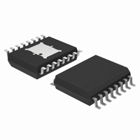
NCV8509PDW18R2G ON Semiconductor, NCV8509PDW18R2G Datasheet - Page 3

NCV8509PDW18R2G
Manufacturer Part Number
NCV8509PDW18R2G
Description
IC REG VOLT DUAL SEQ LIN 16SOIC
Manufacturer
ON Semiconductor
Datasheet
1.NCV8509PDW18R2G.pdf
(18 pages)
Specifications of NCV8509PDW18R2G
Regulator Topology
Positive Fixed
Voltage - Output
3.3V, 1.8V
Voltage - Input
Up to 50V
Voltage - Dropout (typical)
0.4V @ 100mA
Number Of Regulators
2
Current - Limit (min)
115mA, 105mA
Operating Temperature
-40°C ~ 125°C
Mounting Type
Surface Mount
Package / Case
16-SOIC (7.5mm Width) Exposed Pad, 16-eSOIC, 16-HSOIC
Polarity
Positive
Number Of Outputs
2
Output Type
Fixed
Output Voltage
1.8 V, 3.3 V
Output Current
0.115 A, 0.1 A
Line Regulation
50 mV
Load Regulation
50 mV
Dropout Voltage (max)
0.2 V
Input Voltage Max
50 V
Maximum Operating Temperature
+ 125 C
Minimum Operating Temperature
- 40 C
Mounting Style
SMD/SMT
Voltage Regulation Accuracy
2 %
Lead Free Status / RoHS Status
Lead free / RoHS Compliant
Current - Output
-
Lead Free Status / Rohs Status
Lead free / RoHS Compliant
Other names
NCV8509PDW18R2GOS
4. Not a tested parameter.
5. RESET signal sensitive to V
ELECTRICAL CHARACTERISTICS
C
SLEW
RESET
Delay
Output Tracking
Power Shunt
SLEW Charging Current
V
V
SLEW Control Threshold
RESET Threshold Increasing
RESET Threshold Decreasing
RESET Output Low
RESET Output Peak
RESET Threshold Hysteresis
Delay Switching Threshold
Delay Charge Current
Delay Saturation Voltage
Delay Discharge Current
Delta 1 [V
Delta 2 [V
Shunt Voltage 1 (V
Shunt Voltage 2 (V
VOUT1
OUT1
OUT2
(Note 5)
5 V Option
3.3 V Option
2.6 V Option
2.5 V Option
1.8 V Option
5 V Option
3.3 V Option
2.6 V Option
2.5 V Option
1.8 V Option
5 V Option
3.3 V Option
2.6 V Option
2.5 V Option
1.8 V Option
5 V Option
3.3 V Option
SLEW Rate (Note 4)
SLEW Rate
= C
Characteristic
OUT1
OUT2
VOUT2
− V
− V
= 10 mF; unless otherwise noted.)
OUT2
OUT1
IN2
IN2
)
)
]
]
OUT1
and V
SLEW = 1.0 V
C
C
(See Figure 53)
I
Power Down (See Figure 41)
Delay = 1.0 V
V
Delay = 5.0 V V
C
C
C
V
V
RESET
SLEW
SLEW
OUT1
IN1
IN1
OUT1
OUT1
OUT1
OUT2
(continued) (6.0 V < V
= 6.0 V, I
= 12 V, 1.0 mA < I
Out of Regulation
= C
= C
= C
= 33 nF
= 33 nF
= 1.0 mA
.
OUT2
OUT2
OUT2
OUT2
OUT1
, I
, I
, I
Test Conditions
OUT1
OUT1
OUT1
= 100 mA, No R
http://onsemi.com
out of Regulation
OUT2
= I
= I
= I
−
−
−
−
OUT2
OUT2
OUT2
IN1
< 100 mA, No R
3
< 18 V, I
EX
VOUT1
EX
= 5.0 mA, I
1.125
94.5
2.97
2.34
2.25
1.62
3.25
Min
4.0
1.5
4.5
4.0
3.3
50
33
26
25
18
10
−
−
−
−
−
−
−
−
−
−
−
VOUT2
= 5.0 mA, −40°C < T
96.5
4.73
3.12
2.46
2.36
1.70
Typ
710
469
370
355
256
100
6.0
1.8
0.1
0.6
1.5
6.0
4.5
66
52
50
36
−
−
−
−
−
−
0.965 × V
0.965 × V
0.965 × V
0.965 × V
0.965 × V
1.875
Max
98.5
5.75
150
100
8.0
2.1
0.4
1.0
8.0
0.1
3.2
2.8
4.6
99
78
75
54
−
−
−
−
−
−
J
OUT
OUT
OUT
OUT
OUT
< 125°C,
Unit
V/s
V/s
V/s
V/s
V/s
mV
mV
mV
mV
mV
mA
mV
μA
μA
%
V
V
V
V
V
V
V
V
V
V
V
V
V
V


