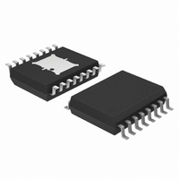
NCV8509PDW18R2G ON Semiconductor, NCV8509PDW18R2G Datasheet - Page 16

NCV8509PDW18R2G
Manufacturer Part Number
NCV8509PDW18R2G
Description
IC REG VOLT DUAL SEQ LIN 16SOIC
Manufacturer
ON Semiconductor
Datasheet
1.NCV8509PDW18R2G.pdf
(18 pages)
Specifications of NCV8509PDW18R2G
Regulator Topology
Positive Fixed
Voltage - Output
3.3V, 1.8V
Voltage - Input
Up to 50V
Voltage - Dropout (typical)
0.4V @ 100mA
Number Of Regulators
2
Current - Limit (min)
115mA, 105mA
Operating Temperature
-40°C ~ 125°C
Mounting Type
Surface Mount
Package / Case
16-SOIC (7.5mm Width) Exposed Pad, 16-eSOIC, 16-HSOIC
Polarity
Positive
Number Of Outputs
2
Output Type
Fixed
Output Voltage
1.8 V, 3.3 V
Output Current
0.115 A, 0.1 A
Line Regulation
50 mV
Load Regulation
50 mV
Dropout Voltage (max)
0.2 V
Input Voltage Max
50 V
Maximum Operating Temperature
+ 125 C
Minimum Operating Temperature
- 40 C
Mounting Style
SMD/SMT
Voltage Regulation Accuracy
2 %
Lead Free Status / RoHS Status
Lead free / RoHS Compliant
Current - Output
-
Lead Free Status / Rohs Status
Lead free / RoHS Compliant
Other names
NCV8509PDW18R2GOS
Slew Rate Control
Control. The diagram highlights the control of one output for
simplicity. V
on−chip current source runing at 6.0 mA (typ.). Charging a
capacitor with a current source creates a linear voltage ramp
as shown in Figure 54.
comparator (Error Amp) dominates the output voltage
(V
power up, it is the dominant factor on the positive terminal
and disables the output. The output (V
linear ramp on the SLEW pin (after being gained up with R1
and R2) until V
occurs when SLEW = V
SLEW
Figure 53 shows the circuitry associated with Slew Rate
The slew rate capacitor (C
The lowest voltage to the positive terminals of the
OUT
C
SLEW
V
V
). Consequently, when C
OUT1
OUT2
Disable Time
Rail ≈ 3.8 V
Internal
Voltage
Figure 53. Slew Control Circuitry
OUT1
Figure 52. Fault Response. Note the High SLEW Rate Coming Out of Fault Conditions.
6.0 μA
BG
and V
Short On
becomes the dominant voltage. This
V
OUT1
V
V
OUT2
IN1
BG
BG
D2
+ V
≈ 10 μs
D1
are both controlled on the IC.
SLEW
SLEW
D1
or approximately 1.8 V.
Decay Time Dependent
on External Load
Soft Start Only Applies to a Power Up Sequence.
) is charged with an
is fully discharged on
+
+
−
Error Amp
OUT
) follows the
Fast SLEW Rate >> Soft Start
http://onsemi.com
R1
R2
V
OUT
Disable Time
16
equation.
182 V/s ON THE SLEW PIN.
by the gain set up by R1 and R2.
assuming V
SLEW pin multiplied by the gain, or:
Slew time can be calculated using the standard capacitor
Using a 33 nF capacitor, the slew time is:
The corresponding slew rate for this is 1.8 V/9.9 ms =
To calculate the slew rate on outputs, you must multiply
For a 5 V output, the gain would be:
The resultant slew rate on the output is the slew rate on the
Short On
V
OUT2
3.8
1.8
BG
(182 V s)
≈ 10 μs
t +
= 1.28 V.
t
SLEW
A v +
I + C dv
(33 nF)(1.8 V)
Decay Time Dependent
on External Load
A v +
1.28 V
Figure 54.
6 mA
dt
5 V
(3.9 V V) + 710 V s
, t +
Time (ms)
Outputs in Regulation
V OUT
1.28 V
Fast SLEW Rate >> Soft Start
+ 3.9 V V
+ 9.9 ms
C(DV)
I


