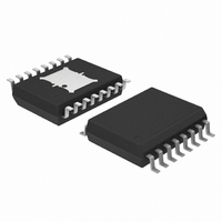
NCV8509PDW18R2G ON Semiconductor, NCV8509PDW18R2G Datasheet - Page 13

NCV8509PDW18R2G
Manufacturer Part Number
NCV8509PDW18R2G
Description
IC REG VOLT DUAL SEQ LIN 16SOIC
Manufacturer
ON Semiconductor
Datasheet
1.NCV8509PDW18R2G.pdf
(18 pages)
Specifications of NCV8509PDW18R2G
Regulator Topology
Positive Fixed
Voltage - Output
3.3V, 1.8V
Voltage - Input
Up to 50V
Voltage - Dropout (typical)
0.4V @ 100mA
Number Of Regulators
2
Current - Limit (min)
115mA, 105mA
Operating Temperature
-40°C ~ 125°C
Mounting Type
Surface Mount
Package / Case
16-SOIC (7.5mm Width) Exposed Pad, 16-eSOIC, 16-HSOIC
Polarity
Positive
Number Of Outputs
2
Output Type
Fixed
Output Voltage
1.8 V, 3.3 V
Output Current
0.115 A, 0.1 A
Line Regulation
50 mV
Load Regulation
50 mV
Dropout Voltage (max)
0.2 V
Input Voltage Max
50 V
Maximum Operating Temperature
+ 125 C
Minimum Operating Temperature
- 40 C
Mounting Style
SMD/SMT
Voltage Regulation Accuracy
2 %
Lead Free Status / RoHS Status
Lead free / RoHS Compliant
Current - Output
-
Lead Free Status / Rohs Status
Lead free / RoHS Compliant
Other names
NCV8509PDW18R2GOS
Why Use a Power Shunt?
power dissipation on the integrated circuit.
dissipates 1.35 W as shown.
into head room issues at 6.0 V and would only be able to
drive 21.5 mA as shown in Figure 45 before causing the
2.5 V output to collapse.
current back in at low voltage operation. So the power is
moved off chip at high voltage where it is needed most.
resistor value (29 Ω) without the power shunt for 6.0 V
operation.
of power is dissipated off chip compared to Figure 44 with
1.35 W.
The power shunt circuitry helps manage and optimize
Figure 44 shows a 100 mA load. A 135 Ω resistor
Without the power shunt, the 135 Ω resistor would run
Figure 46 shows the power shunt circuitry adding the
To further clarify, Figure 47 shows the maximum allowed
Figure 48 shows the scenario at high voltage. Only 290 mW
Figure 44.
R
EX
R
Figure 42. Power Shunt
135 Ω
V
LOAD
OUT2
V
V
IN1
IN2
V
18 V
100 mA
V
4.5 V
V
2.5 V
100 mA
IN1
IN2
OUT2
Regulator
Voltage
http://onsemi.com
+
600 mV
−
R
135 Ω
Figure 45.
LOAD
13
V
6.0 V
21.5 mA
V
3.1 V
V
2.5 V
21.5 mA
IN1
IN2
OUT2
1.8
1.6
1.4
1.2
1.0
0.8
0.6
0.4
0.2
+
600 mV
−
0
R
0
LOAD
29 Ω
Figure 47.
Figure 43. Power On Chip
V
6.0 V
100 mA
V
3.1 V
V
2.5 V
100 mA
IN1
IN2
OUT2
5
R
EX
10
> 138
V
IN
Figure 46.
15
78.5 mA
R
Figure 48.
LOAD
29 Ω
R
R
135 Ω
EX
I
OUT2
LOAD
< 138
R
20
= 100 mA
V
18 V
100 mA
V
15.1 V
V
2.5 V
100 mA
EX
IN1
IN2
OUT2
V
6.0 V
21.5 mA
V
4.5 V
V
2.5 V
100 mA
= 138
IN1
IN2
OUT2
25


