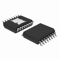
NCV8509PDW18R2G ON Semiconductor, NCV8509PDW18R2G Datasheet - Page 2

NCV8509PDW18R2G
Manufacturer Part Number
NCV8509PDW18R2G
Description
IC REG VOLT DUAL SEQ LIN 16SOIC
Manufacturer
ON Semiconductor
Datasheet
1.NCV8509PDW18R2G.pdf
(18 pages)
Specifications of NCV8509PDW18R2G
Regulator Topology
Positive Fixed
Voltage - Output
3.3V, 1.8V
Voltage - Input
Up to 50V
Voltage - Dropout (typical)
0.4V @ 100mA
Number Of Regulators
2
Current - Limit (min)
115mA, 105mA
Operating Temperature
-40°C ~ 125°C
Mounting Type
Surface Mount
Package / Case
16-SOIC (7.5mm Width) Exposed Pad, 16-eSOIC, 16-HSOIC
Polarity
Positive
Number Of Outputs
2
Output Type
Fixed
Output Voltage
1.8 V, 3.3 V
Output Current
0.115 A, 0.1 A
Line Regulation
50 mV
Load Regulation
50 mV
Dropout Voltage (max)
0.2 V
Input Voltage Max
50 V
Maximum Operating Temperature
+ 125 C
Minimum Operating Temperature
- 40 C
Mounting Style
SMD/SMT
Voltage Regulation Accuracy
2 %
Lead Free Status / RoHS Status
Lead free / RoHS Compliant
Current - Output
-
Lead Free Status / Rohs Status
Lead free / RoHS Compliant
Other names
NCV8509PDW18R2GOS
Stresses exceeding Maximum Ratings may damage the device. Maximum Ratings are stress ratings only. Functional operation above the
Recommended Operating Conditions is not implied. Extended exposure to stresses above the Recommended Operating Conditions may affect
device reliability.
1. 60 second maximum above 183°C.
2. −5°C/+0°C allowable conditions.
3. Both outputs will turn off.
MAXIMUM RATINGS
ELECTRICAL CHARACTERISTICS
C
V
V
General
Output Voltage
Dropout Voltage (V
Load Regulation
Line Regulation
Current Limit
Output Voltage
Load Regulation
Line Regulation
Current Limit
Quiescent Current
Thermal Shutdown (Note 3)
V
V
V
V
Operating Voltage
Input Voltage Range (SLEW, RESET, Delay)
V
V
Electrostatic Discharge (Human Body Model)
Package Thermal Resistance, SOW−16 E Pad:
Lead Temperature Soldering:
OUT1
OUT2
VOUT1
IN1
IN1
IN2
IN2
OUT1
OUT2
5 V Option
3.3 V Option
2.6 V Option
2.5 V Option
1.8 V Option
(dc)
Peak Transient Voltage
(dc)
(Current out of pin)
= C
Characteristic
VOUT2
= 10 mF; unless otherwise noted.)
IN1
− V
OUT1
)
(Machine Model)
1.0 mA < I
1.0 mA < I
I
I
1.0 mA < I
6.0 V < V
V
V
1.0 mA < I
1.0 mA < I
1.0 mA < I
1.0 mA < I
6.0 V < V
V
V
I
I
(Guaranteed by Design)
OUT
OUT
OUT1
OUT1
OUT1
OUT1
OUT2
OUT2
= 100 mA
= 100 μA
(6.0 V < V
= I
= I
= V
= 0 V
= V
= 0 V
OUT2
OUT2
IN1
IN1
VOUT1
VOUT1
VOUT1
VOUT2
VOUT2
VOUT2
VOUT2
Rating
OUT1
OUT2
< 18 V
= V
= 100 μA, V
= 50 mA, V
Junction−to−Case, R
Junction−to−Ambient, R
IN1
(typ) − 500 mV
(typ) − 500 mV
IN2
Test Conditions
< 100 mA
< 100 mA
< 100 mA
< 100 mA
< 100 mA
< 100 mA
< 100 mA
< 18 V, I
< 18 V
http://onsemi.com
IN1
IN1
VOUT1
= 14 V
= 12 V
2
Reflow: (SMD styles only) (Note 1)
= 5.0 mA, I
θJC
θJA
VOUT2
= 5.0 mA, −40°C < T
3.234
2.548
2.450
1.764
Min
115
105
150
4.9
−
−
−
−
−
−
−
−
−
−
Typ
400
100
305
105
305
105
125
180
5.0
3.3
2.6
2.5
1.8
5.0
5.0
10
10
10
240 peak (Note 2)
J
< 125°C,
−0.3 to 50
−0.3 to 10
Value
400
4.0
50
50
10
50
10
10
16
57
3.366
2.652
2.550
1.836
Max
600
200
610
300
610
300
175
210
5.1
50
50
50
50
10
Unit
mV
mV
mV
mV
mA
mA
mV
mV
mA
mA
mA
°C/W
°C/W
μA
Unit
°C
mA
V
V
V
V
V
kV
°C
V
V
V
V
V
V
V
V


