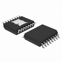
NCV8509PDW18R2G ON Semiconductor, NCV8509PDW18R2G Datasheet - Page 15

NCV8509PDW18R2G
Manufacturer Part Number
NCV8509PDW18R2G
Description
IC REG VOLT DUAL SEQ LIN 16SOIC
Manufacturer
ON Semiconductor
Datasheet
1.NCV8509PDW18R2G.pdf
(18 pages)
Specifications of NCV8509PDW18R2G
Regulator Topology
Positive Fixed
Voltage - Output
3.3V, 1.8V
Voltage - Input
Up to 50V
Voltage - Dropout (typical)
0.4V @ 100mA
Number Of Regulators
2
Current - Limit (min)
115mA, 105mA
Operating Temperature
-40°C ~ 125°C
Mounting Type
Surface Mount
Package / Case
16-SOIC (7.5mm Width) Exposed Pad, 16-eSOIC, 16-HSOIC
Polarity
Positive
Number Of Outputs
2
Output Type
Fixed
Output Voltage
1.8 V, 3.3 V
Output Current
0.115 A, 0.1 A
Line Regulation
50 mV
Load Regulation
50 mV
Dropout Voltage (max)
0.2 V
Input Voltage Max
50 V
Maximum Operating Temperature
+ 125 C
Minimum Operating Temperature
- 40 C
Mounting Style
SMD/SMT
Voltage Regulation Accuracy
2 %
Lead Free Status / RoHS Status
Lead free / RoHS Compliant
Current - Output
-
Lead Free Status / Rohs Status
Lead free / RoHS Compliant
Other names
NCV8509PDW18R2GOS
permissible value of R
package section of the data sheet. Those packages with
Once the value of P
The value of R
Figure 51. 16 Lead SOW (Exposed Pad), qJA as a
100
Thickness), Board Material = 0.0625, G−10/R−4
90
80
70
60
50
40
Function of the Pad Copper Area (2 oz. Cu
0
V
IN1
4.5 V
qJA
R qJA + 150C *
200
can then be compared with those in the
V IN1 t V REF ) V SAT
V IN2 + V IN1 * V SAT
qJA
Copper Area (mm
IC(max)
can be calculated:
Mode 1
P IC
400
is known, the maximum
T A
V
Max V
I(V
IN2
2
)
IN2
600
) × R
IN
Delta
EX
V REF ) V SAT t V IN1 t V REF ) (I OUT2
V IN2 + V REF
Figure 50. V
http://onsemi.com
800
(8)
Mode 2
15
Shunt On
IN
R
the die temperature below 150°C.
dissipate the heat generated by the IC, and an external
heatsink will be required.
Heat Sinks
package to improve the flow of heat away from the IC and
into the surrounding air.
outside environment will have a thermal resistance. Like
series electrical resistances, these resistances are summed to
determine the value of R
where:
R
functions of the package type, heatsink and the interface
between them. These values appear in heat sink data sheets
of heat sink manufacturers.
Shunt
qJA
qJA
In some cases, none of the packages will be sufficient to
A heat sink effectively increases the surface area of the
Each material in the heat flow path between the IC and the
R
R
R
R
qJC
qCS
qSA
qJC
’s less than the calculated value in equation 2 will keep
, it too is a function of package type. R
= the junction−to−case thermal resistance,
appears in the package section of the data sheet. Like
= the case−to−heatsink thermal resistance, and
= the heatsink−to−ambient thermal resistance.
R qJA + R qJC ) R qCS ) R qSA
V IN1 u V REF ) (I OUT2
V IN2 + V IN1 * (I OUT2
Mode 3
qJA
R EX )
:
Shunt Off
R EX )
R EX )
qCS
and R
qSA
are
(9)


