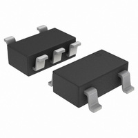
NCP500SN50T1G ON Semiconductor, NCP500SN50T1G Datasheet - Page 5

NCP500SN50T1G
Manufacturer Part Number
NCP500SN50T1G
Description
IC REG LDO 150MA 5.0V LN SOT23-5
Manufacturer
ON Semiconductor
Datasheet
1.NCP500SQL18T1G.pdf
(20 pages)
Specifications of NCP500SN50T1G
Regulator Topology
Positive Fixed
Voltage - Output
5V
Voltage - Input
Up to 6V
Voltage - Dropout (typical)
0.12V @ 150mA
Number Of Regulators
1
Current - Output
150mA
Operating Temperature
-40°C ~ 85°C
Mounting Type
Surface Mount
Package / Case
TSOT-23-5, TSOT-5, TSOP-5
Number Of Outputs
1
Polarity
Positive
Input Voltage Max
6 V
Output Voltage
5 V
Output Type
Fixed
Dropout Voltage (max)
0.01 V at 1 mA
Output Current
150 mA
Line Regulation
10 mV
Load Regulation
45 mV
Voltage Regulation Accuracy
2.5 %
Maximum Operating Temperature
+ 125 C
Mounting Style
SMD/SMT
Lead Free Status / RoHS Status
Lead free / RoHS Compliant
Current - Limit (min)
-
Lead Free Status / Rohs Status
Lead free / RoHS Compliant
Other names
NCP500SN50T1GOS
Available stocks
Company
Part Number
Manufacturer
Quantity
Price
Company:
Part Number:
NCP500SN50T1G
Manufacturer:
ON
Quantity:
45 000
Part Number:
NCP500SN50T1G
Manufacturer:
ON/安森美
Quantity:
20 000
ELECTRICAL CHARACTERISTICS
values T
−2.8 V
ELECTRICAL CHARACTERISTICS
values T
−3.0 V
Output Voltage
Line Regulation (V
Load Regulation (I
Dropout Voltage (Measured at V
Output Short Circuit Current
Ripple Rejection
Quiescent Current
Enable Input Threshold Voltage
Enable Input Bias Current
Output Turn On Time (Enable Input = 0 V to V
Output Voltage
Line Regulation (V
Load Regulation (I
Dropout Voltage (Measured at V
Output Short Circuit Current
Ripple Rejection
Quiescent Current
Enable Input Threshold Voltage
Enable Input Bias Current
Output Turn On Time (Enable Input = 0 V to V
(T
(Iout = 1.0 mA)
(Iout = 75 mA)
(Iout = 150 mA)
(V
(Enable Input = 0 V)
(Enable Input = 0.9 V, I
(Enable Input = 0.9 V, I
(Voltage Increasing, Output Turns On, Logic High)
(Voltage Decreasing, Output Turns Off, Logic Low)
(T
(Iout = 1.0 mA)
(Iout = 75 mA)
(Iout = 150 mA)
(V
(Enable Input = 0 V)
(Enable Input = 0.9 V, I
(Enable Input = 0.9 V, I
(Voltage Increasing, Output Turns On, Logic High)
(Voltage Decreasing, Output Turns Off, Logic Low)
A
A
in
in
=−40°C to 85°C, I
=−40°C to 85°C, I
= V
= V
A
A
= −40°C to 85°C, T
= −40°C to 85°C, T
out (nom.)
out (nom.)
out
out
in
in
+ 1.0 V + 0.5 V
+ 1.0 V + 0.5 V
= 3.3 V to 6.0 V, I
= 3.5 V to 6.0 V, I
= 1.0 mA to 150 mA)
= 1.0 mA to 150 mA)
out
out
out
out
out
out
= 1.0 mA to 150 mA)
= 1.0 mA to 150 mA)
Characteristic
= 1.0 mA)
= 150 mA)
Characteristic
= 1.0 mA)
= 150 mA)
jmax
jmax
out
out
= 125°C, unless otherwise noted)
= 125°C, unless otherwise noted)
pp
pp
−
−
2.0%, T
2.0%, T
, f = 1.0 kHz, I
, f = 1.0 kHz, I
out
out
= 1.0 mA)
= 1.0 mA)
(V
(V
A
A
in
in
= −40°C to 85°C)
= −40°C to 85°C)
in
in
= 3.3 V, C
= 3.5 V, C
)
)
o
o
= 60 mA)
= 60 mA)
http://onsemi.com
in
in
= 1.0 mF, C
= 1.0 mF, C
NCP500
5
out
out
Symbol
Symbol
V
V
Reg
I
Reg
I
Reg
Reg
= 1.0 mF, for typical value T
V
= 1.0 mF, for typical value T
V
out(max)
out(max)
I
I
in
in
IB(EN)
IB(EN)
V
V
RR
th(EN)
RR
th(EN)
−
I
−
I
−
−
out
out
Q
Q
V
V
load
load
line
line
out
out
2.730
2.925
Min
200
Min
200
0.9
0.9
−
−
−
−
−
−
−
−
−
−
−
−
−
−
−
−
−
−
−
−
−
−
−
−
0.01
0.01
Typ
170
540
185
185
Typ
165
540
190
190
2.8
1.0
2.0
3.0
3.0
1.0
2.0
3.0
15
90
62
20
15
85
62
20
−
−
−
−
A
A
= 25°C, for min and max
= 25°C, for min and max
2.870
3.075
Max
0.15
Max
0.15
150
250
700
300
300
100
100
130
240
700
300
300
100
100
1.0
1.0
10
45
10
10
45
10
−
−
−
−
Unit
Unit
mV
mV
mV
mA
mV
mV
mV
mA
dB
nA
dB
nA
mA
mA
ms
ms
V
V
V
V


