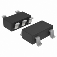
NCP500SN50T1G ON Semiconductor, NCP500SN50T1G Datasheet - Page 4

NCP500SN50T1G
Manufacturer Part Number
NCP500SN50T1G
Description
IC REG LDO 150MA 5.0V LN SOT23-5
Manufacturer
ON Semiconductor
Datasheet
1.NCP500SQL18T1G.pdf
(20 pages)
Specifications of NCP500SN50T1G
Regulator Topology
Positive Fixed
Voltage - Output
5V
Voltage - Input
Up to 6V
Voltage - Dropout (typical)
0.12V @ 150mA
Number Of Regulators
1
Current - Output
150mA
Operating Temperature
-40°C ~ 85°C
Mounting Type
Surface Mount
Package / Case
TSOT-23-5, TSOT-5, TSOP-5
Number Of Outputs
1
Polarity
Positive
Input Voltage Max
6 V
Output Voltage
5 V
Output Type
Fixed
Dropout Voltage (max)
0.01 V at 1 mA
Output Current
150 mA
Line Regulation
10 mV
Load Regulation
45 mV
Voltage Regulation Accuracy
2.5 %
Maximum Operating Temperature
+ 125 C
Mounting Style
SMD/SMT
Lead Free Status / RoHS Status
Lead free / RoHS Compliant
Current - Limit (min)
-
Lead Free Status / Rohs Status
Lead free / RoHS Compliant
Other names
NCP500SN50T1GOS
Available stocks
Company
Part Number
Manufacturer
Quantity
Price
Company:
Part Number:
NCP500SN50T1G
Manufacturer:
ON
Quantity:
45 000
Part Number:
NCP500SN50T1G
Manufacturer:
ON/安森美
Quantity:
20 000
ELECTRICAL CHARACTERISTICS
values T
−2.6 V
ELECTRICAL CHARACTERISTICS
values T
−2.7 V
Output Voltage
Line Regulation (V
Load Regulation (I
Dropout Voltage (Measured at V
Output Short Circuit Current
Ripple Rejection
Quiescent Current
Enable Input Threshold Voltage
Enable Input Bias Current
Output Turn On Time (Enable Input = 0 V to V
Output Voltage
Line Regulation (V
Load Regulation (I
Dropout Voltage (Measured at V
Output Short Circuit Current
Ripple Rejection
Quiescent Current
Enable Input Threshold Voltage
Enable Input Bias Current
Output Turn On Time (Enable Input = 0 V to V
(T
(Iout = 1.0 mA)
(Iout = 75 mA)
(Iout = 150 mA)
(V
(Enable Input = 0 V)
(Enable Input = 0.9 V, I
(Enable Input = 0.9 V, I
(Voltage Increasing, Output Turns On, Logic High)
(Voltage Decreasing, Output Turns Off, Logic Low)
(T
(Iout = 1.0 mA)
(Iout = 75 mA)
(Iout = 150 mA)
(V
(Enable Input = 0 V)
(Enable Input = 0.9 V, I
(Enable Input = 0.9 V, I
(Voltage Increasing, Output Turns On, Logic High)
(Voltage Decreasing, Output Turns Off, Logic Low)
A
A
in
in
=−40°C to 85°C, I
=−40°C to 85°C, I
= V
= V
A
A
= −40°C to 85°C, T
= −40°C to 85°C, T
out (nom.)
out (nom.)
out
out
in
in
+ 1.0 V + 0.5 V
+ 1.0 V + 0.5 V
= 3.0 V to 6.0 V, I
= 3.2 V to 6.0 V, I
= 1.0 mA to 150 mA)
= 1.0 mA to 150 mA)
out
out
out
out
out
out
= 1.0 mA to 150 mA)
= 1.0 mA to 150 mA)
Characteristic
= 1.0 mA)
= 150 mA)
Characteristic
= 1.0 mA)
= 150 mA)
jmax
jmax
out
out
= 125°C, unless otherwise noted)
= 125°C, unless otherwise noted)
pp
pp
−
−
2.0%, T
2.0%, T
, f = 1.0 kHz, I
, f = 1.0 kHz, I
out
out
= 1.0 mA)
= 1.0 mA)
(V
(V
A
A
in
in
= −40°C to 85°C)
= −40°C to 85°C)
in
in
= 3.1 V, C
= 3.2 V, C
)
)
o
o
= 60 mA)
= 60 mA)
http://onsemi.com
in
in
= 1.0 mF, C
= 1.0 mF, C
NCP500
4
out
out
Symbol
Symbol
V
V
Reg
I
Reg
I
Reg
Reg
= 1.0 mF, for typical value T
V
= 1.0 mF, for typical value T
V
out(max)
out(max)
I
I
in
in
IB(EN)
IB(EN)
V
V
RR
th(EN)
RR
th(EN)
−
−
I
I
−
−
out
Q
out
Q
V
V
load
load
line
line
out
out
2.535
2.633
Min
200
Min
200
0.9
0.9
−
−
−
−
−
−
−
−
−
−
−
−
−
−
−
−
−
−
−
−
−
−
−
−
0.01
0.01
Typ
540
180
180
Typ
180
540
185
185
2.6
1.0
2.0
3.0
2.7
1.0
2.0
3.0
15
62
20
15
90
62
20
−
−
−
−
−
−
A
A
= 25°C, for min and max
= 25°C, for min and max
2.665
2.768
Max
0.15
Max
0.15
700
300
300
100
100
160
260
700
300
300
100
100
1.0
1.0
10
45
10
10
45
10
−
−
−
−
−
−
Unit
Unit
mV
mV
mV
mA
mV
mV
mV
mA
dB
nA
dB
nA
mA
mA
ms
ms
V
V
V
V


