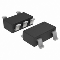
NCP500SN50T1G ON Semiconductor, NCP500SN50T1G Datasheet

NCP500SN50T1G
Specifications of NCP500SN50T1G
Available stocks
Related parts for NCP500SN50T1G
NCP500SN50T1G Summary of contents
Page 1
NCP500 150 mA CMOS Low Noise Low−Dropout Voltage Regulator The NCP500 series of fixed output low dropout linear regulators are designed for portable battery powered applications which require low noise operation, fast enable response time, and low dropout. The device ...
Page 2
PIN FUNCTION DESCRIPTION Á Á Á Á ...
Page 3
ELECTRICAL CHARACTERISTICS (continued) (V max values T = −40°C to 85° 125°C, unless otherwise noted) A jmax Output Turn On Time (Enable Input = Characteristic −1.85 V Output Voltage (T = −40°C to 85°C, ...
Page 4
ELECTRICAL CHARACTERISTICS values T = −40°C to 85° 125°C, unless otherwise noted) A jmax Characteristic −2.6 V Output Voltage (T =−40°C to 85° 1 150 mA) A out Line Regulation (V = 3.0 V ...
Page 5
ELECTRICAL CHARACTERISTICS values T = −40°C to 85° 125°C, unless otherwise noted) A jmax Characteristic −2.8 V Output Voltage (T =−40°C to 85° 1 150 mA) A out Line Regulation (V = 3.3 V ...
Page 6
ELECTRICAL CHARACTERISTICS values T = −40°C to 85° 125°C, unless otherwise noted) A jmax Characteristic −3.3 V Output Voltage (T =−40°C to 85° 1 150 mA) A out Line Regulation (V = 3.8 V ...
Page 7
ELECTRICAL CHARACTERISTICS values T = −40°C to 85° 125°C, unless otherwise noted) A jmax Characteristic −5.0 V Output Voltage (T =−40°C to 85° 1 150 mA) A out Line Regulation (V = 5.5 V ...
Page 8
V = 3.3 V out(nom Load Load 10 1.0 mA Load 0 −50 − Temperature (°C) Figure 2. Dropout Voltage vs. Temperature 2.8 V ...
Page 9
+0 out(nom.) 3.306 V = 3.3 V out(nom 1 3.304 3.302 3.300 3.298 3.296 3.294 3.292 −50 − Temperature (°C) Figure 8. Output Voltage vs. Temperature 1.804 ...
Page 10
V out(nom.) I out 1.0 2.0 3.0 Input Voltage (V) Figure 14. Ground Pin Current vs. Input Voltage 600 500 400 300 200 100 V out(nom.) 0 ...
Page 11
V in 150 V out C out 100 I out 50 0 − 100 Time (ms) Figure 20. Line Transient Response 225 150 −25 −50 0 ...
Page 12
C 0 out 0 0.2 Enable Input Voltage (V) in, Figure 24. Output Voltage vs. Input Voltage 3.5 3 2.5 2 1.5 ...
Page 13
Load Regulation The change in output voltage for a change in output load current at a constant temperature. Dropout Voltage The input/output differential at which the regulator output no longer maintains regulation against further reductions in input voltage. Measured when ...
Page 14
The NCP500 series regulators are protected with internal thermal shutdown and internal current limit. A typical application circuit is shown in Figure 27. Input Decoupling (C1) A 1.0 mF capacitor either ceramic or tantalum is recommended and should be connected ...
Page 15
Battery or Unregulated 1 + Voltage OFF Figure 27. Typical Application Circuit 10 1 0.1 0.01 0 Input 1 Figure 30. Current Boost Regulator The NCP500 series can be current ...
Page 16
Input 1 1 Enable Figure 32. Delayed Turn− delayed turn−on is needed during power up of several volt- ages then the above schematic can be used. Resistor R, ...
Page 17
... NCP500SN185T1 NCP500SN185T1G NCP500SN25T1 NCP500SN25T1G NCP500SN26T1 NCP500SN26T1G NCP500SN27T1 NCP500SN27T1G NCP500SN28T1 NCP500SN28T1G NCP500SN30T1 NCP500SN30T1G NCP500SN33T1 NCP500SN33T1G NCP500SN50T1 NCP500SN50T1G NCP500SQL18T1 NCP500SQL18T1G NCP500SQL25T1 NCP500SQL25T1G NCP500SQL27T1 NCP500SQL27T1G NCP500SQL28T1 NCP500SQL28T1G NCP500SQL30T1 NCP500SQL30T1G NCP500SQL33T1 NCP500SQL33T1G NCP500SQL50T1 NCP500SQL50T1G For availability of other output voltages, please contact your local ON Semiconductor Sales Representative. ...
Page 18
... C 0.05 (0.002) H SOLDERING FOOTPRINT* 0.95 0.037 1.0 0.039 *For additional information on our Pb−Free strategy and soldering details, please download the ON Semiconductor Soldering and Mounting Techniques Reference Manual, SOLDERRM/D. http://onsemi.com NCP500 TSOP−5 SN SUFFIX CASE 483−02 ISSUE E NOTES: 1. DIMENSIONING AND TOLERANCING PER ANSI Y14 ...
Page 19
... 0.05 C NOTE 3 *For additional information on our Pb−Free strategy and soldering details, please download the ON Semiconductor Soldering and Mounting Techniques Reference Manual, SOLDERRM/D. EXPOSED Cu É É É A3 É É É DETAIL B Side View (Optional) http://onsemi.com 19 NOTES: 1 ...
Page 20
... Fax: 480−829−7709 or 800−344−3867 Toll Free USA/Canada Email: orderlit@onsemi.com NCP500 N. American Technical Support: 800−282−9855 Toll Free USA/Canada Japan: ON Semiconductor, Japan Customer Focus Center 2−9−1 Kamimeguro, Meguro−ku, Tokyo, Japan 153−0051 Phone: 81−3−5773−3850 http://onsemi.com 20 ON Semiconductor Website: http://onsemi ...


