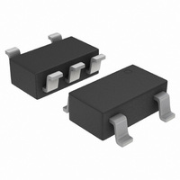
NCP500SN50T1G ON Semiconductor, NCP500SN50T1G Datasheet - Page 15

NCP500SN50T1G
Manufacturer Part Number
NCP500SN50T1G
Description
IC REG LDO 150MA 5.0V LN SOT23-5
Manufacturer
ON Semiconductor
Datasheet
1.NCP500SQL18T1G.pdf
(20 pages)
Specifications of NCP500SN50T1G
Regulator Topology
Positive Fixed
Voltage - Output
5V
Voltage - Input
Up to 6V
Voltage - Dropout (typical)
0.12V @ 150mA
Number Of Regulators
1
Current - Output
150mA
Operating Temperature
-40°C ~ 85°C
Mounting Type
Surface Mount
Package / Case
TSOT-23-5, TSOT-5, TSOP-5
Number Of Outputs
1
Polarity
Positive
Input Voltage Max
6 V
Output Voltage
5 V
Output Type
Fixed
Dropout Voltage (max)
0.01 V at 1 mA
Output Current
150 mA
Line Regulation
10 mV
Load Regulation
45 mV
Voltage Regulation Accuracy
2.5 %
Maximum Operating Temperature
+ 125 C
Mounting Style
SMD/SMT
Lead Free Status / RoHS Status
Lead free / RoHS Compliant
Current - Limit (min)
-
Lead Free Status / Rohs Status
Lead free / RoHS Compliant
Other names
NCP500SN50T1GOS
Available stocks
Company
Part Number
Manufacturer
Quantity
Price
Company:
Part Number:
NCP500SN50T1G
Manufacturer:
ON
Quantity:
45 000
Part Number:
NCP500SN50T1G
Manufacturer:
ON/安森美
Quantity:
20 000
Unregulated
Battery or
Input
Voltage
The NCP500 series can be current boosted with a PNP transis-
tor. Resistor R in conjunction with V
when the pass transistor begins conducting; this circuit is not
short circuit proof. Input/Output differential voltage minimum is
increased by V
OFF
R
1.0 mF
ON
Figure 30. Current Boost Regulator
Figure 27. Typical Application Circuit
Q1
BE
C1
of the pass resistor.
+
1
2
3
1
2
3
0.01
0.1
BE
10
1
of the PNP determines
0
5
4
5
4
UNSTABLE
STABLE
25
1.0 mF
Output
http://onsemi.com
+
I
O,
50
Figure 29. Stability
C2
V
out
Output Current (mA)
Input
NCP500
Q2
15
75
Unregulated
Battery or
Short circuit current limit is essentially set by the V
R1. I
OFF
Voltage
Figure 31. Current Boost Regulator with Short
C
T
V
R1
R2
A
SC
out
in
100
ON
= 40°C to 125°C
= up to 6.0 V
= ((V
= 1 mF to 10 mF
Figure 28. Typical Application Circuit
BEQ2
1.0 mF
C1
R3
125
+
− ib * R2) / R1) + I
Q1
Circuit Limit
150
1
2
3
1
2
3
O(max) Regulator
6
5
4
5
4
BE
of Q2 and
1.0 mF
+
C2
Output
V
out


