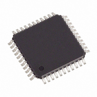
DS89C420-ENG Maxim Integrated Products, DS89C420-ENG Datasheet - Page 3

DS89C420-ENG
Manufacturer Part Number
DS89C420-ENG
Description
IC MCU ULTRA 25MHZ HP 44-TQFP
Manufacturer
Maxim Integrated Products
Series
89Cr
Datasheet
1.DS89C420-QCS.pdf
(47 pages)
Specifications of DS89C420-ENG
Core Processor
8051
Core Size
8-Bit
Speed
25MHz
Connectivity
EBI/EMI, SIO, UART/USART
Peripherals
Power-Fail Reset, WDT
Number Of I /o
32
Program Memory Size
16KB (16K x 8)
Program Memory Type
FLASH
Ram Size
1K x 8
Voltage - Supply (vcc/vdd)
4.5 V ~ 5.5 V
Oscillator Type
External
Operating Temperature
-40°C ~ 85°C
Package / Case
44-TQFP, 44-VQFP
Lead Free Status / RoHS Status
Contains lead / RoHS non-compliant
Eeprom Size
-
Data Converters
-
Available stocks
Company
Part Number
Manufacturer
Quantity
Price
Company:
Part Number:
DS89C420-ENG
Manufacturer:
Maxim Integrated
Quantity:
10 000
Note 1: Specifications to -40°C are guaranteed by design and not production tested.
Note 2: All voltages are referenced to ground.
Note 3: Active current is measured with a 25MHz/33MHz clock source driving XTAL1, V
Note 4: Idle mode current measured with a 25MHz/33MHz clock source driving XTAL1, V
Note 5: Stop mode measured with XTAL and RST grounded, V
Note 6: When addressing external memory.
Note 7: RST = 5.5V. This condition mimics the operation of pins in I/O mode.
Note 8: During a 0-to-1 transition, a one-shot drives the ports hard for two clock cycles. This measurement reflects a port pin in transition mode.
Note 9: Ports 1, 2, and 3 source transition current when being pulled down externally. The current reaches its maximum at approximately 2V.
Note 10: This port is a weak address holding latch in bus mode. Peak current occurs near the input transition point of the holding latch at
Note 11: RST = 5.5V. Port 0 floating during reset and when in the logic-high state during I/O mode.
Note 12: While the specifications for V
Note 13: The user should note that this part is tested and guaranteed to operate down to 4.5V (10%) and that V
Note 14: Guaranteed by design.
approximately 2V.
given, there is a guaranteed separation between these two voltages.
point. This indicates that there is a range of voltages [V
reset trip point has not been reached. This should not be an issue in most applications, but should be considered when proper
operation must be maintained at all times. For these applications, it may be desirable to use a more accurate external reset.
PFW
and V
RST
overlap, the design of the hardware makes it such that this is not possible. Within the ranges
CC
3 of 47
= 5.5V. All other pins disconnected.
MIN
to V
RST
(min)] where the processor’s operation is not guaranteed, but the
CC
CC
= RST = 5.5V. All other pins disconnected.
= 5.5V, RST at ground. All other pins disconnected.
RST
(min) is specified below that


