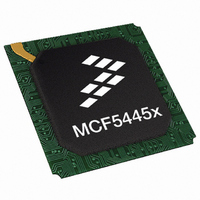
MCF54455CVR200 Freescale Semiconductor, MCF54455CVR200 Datasheet - Page 33

MCF54455CVR200
Manufacturer Part Number
MCF54455CVR200
Description
IC MPU 32BIT 200MHZ 360TEPBGA
Manufacturer
Freescale Semiconductor
Series
MCF5445xr
Datasheet
1.MCF54452CVR200.pdf
(48 pages)
Specifications of MCF54455CVR200
Core Processor
Coldfire V4
Core Size
32-Bit
Speed
200MHz
Connectivity
I²C, SPI, SSI, UART/USART, USB OTG
Peripherals
DMA, WDT
Number Of I /o
132
Program Memory Type
ROMless
Ram Size
32K x 8
Voltage - Supply (vcc/vdd)
1.35 V ~ 3.6 V
Oscillator Type
Internal
Operating Temperature
-40°C ~ 85°C
Package / Case
360-TEPBGA
Processor Series
MCF544x
Core
ColdFire V4
Data Bus Width
32 bit
Program Memory Size
16 KB
Data Ram Size
32 KB
Interface Type
I2C, SPI, SSI
Maximum Clock Frequency
66 MHz
Number Of Timers
8
Operating Supply Voltage
- 0.3 V to + 4 V
Maximum Operating Temperature
+ 85 C
Mounting Style
SMD/SMT
3rd Party Development Tools
JLINK-CF-BDM26, EWCF
Development Tools By Supplier
M54455EVB
Minimum Operating Temperature
- 40 C
On-chip Adc
16 bit, 16 Channel
On-chip Dac
16 bit, 16 Channel
Leaded Process Compatible
Yes
Rohs Compliant
Yes
Peak Reflow Compatible (260 C)
Yes
For Use With
M54455EVB - BOARD EVAL FOR MCF5445X
Lead Free Status / RoHS Status
Lead free / RoHS Compliant
Eeprom Size
-
Program Memory Size
-
Data Converters
-
Lead Free Status / Rohs Status
Lead free / RoHS Compliant
Available stocks
Company
Part Number
Manufacturer
Quantity
Price
Company:
Part Number:
MCF54455CVR200
Manufacturer:
Freescale Semiconductor
Quantity:
135
Company:
Part Number:
MCF54455CVR200
Manufacturer:
FREESCAL
Quantity:
624
5.13
The following timing specs are defined at the chip I/O pin and must be translated appropriately to arrive at timing
specs/constraints for the physical interface.
5.13.1
The following timing specs meet the requirements for MII and 7-Wire style interfaces for a range of transceiver devices.
Freescale Semiconductor
1
In MII mode, n = 3; In RMII mode, n = 1
Num
E1
E2
E3
E4
1
2
3
I2C_SDA
—
I2C_SCL
Num
Output numbers depend on the value programmed into the IFDR; an IFDR programmed with the maximum
frequency (IFDR = 0x20) results in minimum output timings as shown in
designed to scale the actual data transition time to move it to the middle of the SCL low period. The actual
position is affected by the prescale and division values programmed into the IFDR. However, the numbers
given in
Because I2C_SCL and I2C_SDA are open-collector-type outputs, which the processor can only actively drive
low, the time I2C_SCL or I2C_SDA take to reach a high level depends on external signal capacitance and
pull-up resistor values.
Specified at a nominal 50-pF load.
I6
I7
I8
I9
Fast Ethernet Timing Specifications
1
1
1
1
Receive Signal Timing Specifications
RXCLK frequency
RXD[n:0], RXDV, RXER to RXCLK setup
RXCLK to RXD[n:0], RXDV, RXER hold
RXCLK pulse width high
RXCLK pulse width low
Table 19. I
Clock high time
Data setup time
Start condition setup time (for repeated start condition only)
Stop condition setup time
Table 19
I1
are minimum values.
2
Characteristic
C Output Timing Specifications between SCL and SDA (continued)
MCF5445x ColdFire
I2
Characteristic
Figure 18. I
Table 20. Receive Signal Timing
I4
1
®
2
1
Microprocessor Data Sheet, Rev. 6
C Input/Output Timings
I6
35%
35%
Min
—
5
5
MII Mode
I7
Max
65%
65%
25
—
—
Table
Min
I8
10
20
10
35%
35%
Min
2
—
4
2
RMII Mode
19. The I
I5
Max
I3
—
—
—
—
Max
65%
65%
50
—
—
2
C interface is
Electrical Characteristics
RXCLK period
RXCLK period
Units
t
t
t
t
SYS
SYS
SYS
SYS
MHz
Unit
ns
ns
I9
33


