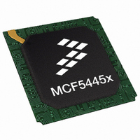
MCF54455CVR200 Freescale Semiconductor, MCF54455CVR200 Datasheet - Page 30

MCF54455CVR200
Manufacturer Part Number
MCF54455CVR200
Description
IC MPU 32BIT 200MHZ 360TEPBGA
Manufacturer
Freescale Semiconductor
Series
MCF5445xr
Datasheet
1.MCF54452CVR200.pdf
(48 pages)
Specifications of MCF54455CVR200
Core Processor
Coldfire V4
Core Size
32-Bit
Speed
200MHz
Connectivity
I²C, SPI, SSI, UART/USART, USB OTG
Peripherals
DMA, WDT
Number Of I /o
132
Program Memory Type
ROMless
Ram Size
32K x 8
Voltage - Supply (vcc/vdd)
1.35 V ~ 3.6 V
Oscillator Type
Internal
Operating Temperature
-40°C ~ 85°C
Package / Case
360-TEPBGA
Processor Series
MCF544x
Core
ColdFire V4
Data Bus Width
32 bit
Program Memory Size
16 KB
Data Ram Size
32 KB
Interface Type
I2C, SPI, SSI
Maximum Clock Frequency
66 MHz
Number Of Timers
8
Operating Supply Voltage
- 0.3 V to + 4 V
Maximum Operating Temperature
+ 85 C
Mounting Style
SMD/SMT
3rd Party Development Tools
JLINK-CF-BDM26, EWCF
Development Tools By Supplier
M54455EVB
Minimum Operating Temperature
- 40 C
On-chip Adc
16 bit, 16 Channel
On-chip Dac
16 bit, 16 Channel
Leaded Process Compatible
Yes
Rohs Compliant
Yes
Peak Reflow Compatible (260 C)
Yes
For Use With
M54455EVB - BOARD EVAL FOR MCF5445X
Lead Free Status / RoHS Status
Lead free / RoHS Compliant
Eeprom Size
-
Program Memory Size
-
Data Converters
-
Lead Free Status / Rohs Status
Lead free / RoHS Compliant
Available stocks
Company
Part Number
Manufacturer
Quantity
Price
Company:
Part Number:
MCF54455CVR200
Manufacturer:
Freescale Semiconductor
Quantity:
135
Company:
Part Number:
MCF54455CVR200
Manufacturer:
FREESCAL
Quantity:
624
Electrical Characteristics
5.11
This section provides the AC timings for the SSI in master (clocks driven) and slave modes (clocks input). All timings are given
for non-inverted serial clock polarity (SSI_TCR[TSCKP] = 0, SSI_RCR[RSCKP] = 0) and a non-inverted frame sync
(SSI_TCR[TFSI] = 0, SSI_RCR[RFSI] = 0). If the polarity of the clock and/or the frame sync have been inverted, all the timings
remain valid by inverting the clock signal (SSI_BCLK) and/or the frame sync (SSI_FS) shown in the figures below.
30
1
2
3
Num
S10
All timings specified with a capactive load of 25pF.
SSI_MCLK can be generated from SSI_CLKIN or a divided version of the internal system clock (f
SSI_BCLK can be derived from SSI_CLKIN or a divided version of the internal system clock (f
S1
S2
S3
S4
S5
S6
S7
S8
S9
SSI Timing Specifications
SSI_MCLK cycle time
SSI_MCLK pulse width high / low
SSI_BCLK cycle time
SSI_BCLK pulse width
SSI_BCLK to SSI_FS output valid
SSI_BCLK to SSI_FS output invalid
SSI_BCLK to SSI_TXD valid
SSI_BCLK to SSI_TXD invalid / high impedence
SSI_RXD / SSI_FS input setup before SSI_BCLK
SSI_RXD / SSI_FS input hold after SSI_BCLK
ULPI_DIR / ULPI_NXT
ULPI_DATA[7:0]
(Control Output)
ULPI_DATA[7:0]
(Control Input)
(Data Output)
USB_CLKIN
(Data Input)
ULPI_STP
MCF5445x ColdFire
Description
Table 16. SSI Timing — Master Modes
Figure 15. ULPI Timing Diagram
U2
U2
®
Microprocessor Data Sheet, Rev. 6
U3
U3
U4
U4
Symbol
t
t
MCLK
BCLK
U1
2 × t
8 × t
45%
45%
Min
10
—
—
1
-2
0
0
SYS
SYS
U5
U5
55%
55%
Max
15
15
—
—
—
—
—
—
sys
Freescale Semiconductor
).
sys
Units
t
t
MCLK
BCLK
ns
ns
ns
ns
ns
ns
ns
ns
).
Notes
2
3


