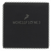
MCHC11F1CFNE3 Freescale Semiconductor, MCHC11F1CFNE3 Datasheet - Page 88

MCHC11F1CFNE3
Manufacturer Part Number
MCHC11F1CFNE3
Description
IC MCU 8BIT 1K RAM 68-PLCC
Manufacturer
Freescale Semiconductor
Series
HC11r
Specifications of MCHC11F1CFNE3
Core Processor
HC11
Core Size
8-Bit
Speed
3MHz
Connectivity
SCI, SPI
Peripherals
POR, WDT
Number Of I /o
30
Program Memory Type
ROMless
Eeprom Size
512 x 8
Ram Size
1K x 8
Voltage - Supply (vcc/vdd)
4.75 V ~ 5.25 V
Data Converters
A/D 8x8b
Oscillator Type
Internal
Operating Temperature
-40°C ~ 85°C
Package / Case
68-PLCC
A/d Inputs
8-Channel, 8-Bit
Eeprom Memory
512 Bytes
Input Output
30
Interface
SCI/SPI
Memory Type
EPROM
Number Of Bits
8
Package Type
68-pin PLCC
Programmable Memory
0 Bytes
Timers
3-16-bit
Voltage, Range
3-5.5 V
Controller Family/series
68HC11
No. Of I/o's
30
Eeprom Memory Size
512Byte
Ram Memory Size
1KB
Cpu Speed
3MHz
No. Of Timers
1
Embedded Interface Type
SCI, SPI
Rohs Compliant
Yes
Processor Series
HC11F
Core
HC11
Data Bus Width
8 bit
Program Memory Size
512 B
Data Ram Size
1 KB
Interface Type
SCI, SPI
Maximum Clock Frequency
3 MHz
Number Of Timers
1
Maximum Operating Temperature
+ 85 C
Mounting Style
SMD/SMT
Minimum Operating Temperature
- 40 C
On-chip Adc
8 bit, 8 Channel
Lead Free Status / RoHS Status
Lead free / RoHS Compliant
Program Memory Size
-
Lead Free Status / Rohs Status
RoHS Compliant part
Available stocks
Company
Part Number
Manufacturer
Quantity
Price
Company:
Part Number:
MCHC11F1CFNE3
Manufacturer:
FREESCALE
Quantity:
5 530
Company:
Part Number:
MCHC11F1CFNE3
Manufacturer:
FREESCALE
Quantity:
5 530
Company:
Part Number:
MCHC11F1CFNE3
Manufacturer:
Freescale Semiconductor
Quantity:
10 000
Company:
Part Number:
MCHC11F1CFNE3R
Manufacturer:
Freescale Semiconductor
Quantity:
10 000
7.3 Receive Operation
7-2
REQUESTS
TRANSMITTER
During receive operations, the transmit sequence is reversed. The serial shift register
receives data and transfers it to a parallel receive data register (SCDR) as a complete
word. This double buffered operation allows a character to be shifted in serially while
another character is already in the SCDR. An advanced data recovery scheme distin-
guishes valid data from noise in the serial data stream. The data input is selectively
sampled to detect receive data, and a majority voting circuit determines the value and
integrity of each bit.
BAUD RATE
SCI Rx
CLOCK
SCCR1 SCI CONTROL 1
SCI INTERRUPT
REQUEST
H (8) 7 6 5 4 3 2 1 0
10 (11) - BIT Tx SHIFT REGISTER
Figure 7-1 SCI Transmitter Block Diagram
Freescale Semiconductor, Inc.
SCDR Tx BUFFER
For More Information On This Product,
SERIAL COMMUNICATIONS INTERFACE
TDRE
TIE
TC
TCIE
CONTROL LOGIC
Go to: www.freescale.com
TRANSMITTER
SCSR INTERRUPT STATUS
L
(WRITE-ONLY)
SCCR2 SCI CONTROL 2
DIRECTION (OUT)
FORCE PIN
8
AND CONTROL
PIN BUFFER
8
DDD1
INTERNAL
DATA BUS
8
8
TECHNICAL DATA
MC68HC11F1
PD1/
TxD


