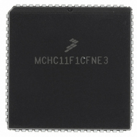
MCHC11F1CFNE3 Freescale Semiconductor, MCHC11F1CFNE3 Datasheet - Page 73

MCHC11F1CFNE3
Manufacturer Part Number
MCHC11F1CFNE3
Description
IC MCU 8BIT 1K RAM 68-PLCC
Manufacturer
Freescale Semiconductor
Series
HC11r
Specifications of MCHC11F1CFNE3
Core Processor
HC11
Core Size
8-Bit
Speed
3MHz
Connectivity
SCI, SPI
Peripherals
POR, WDT
Number Of I /o
30
Program Memory Type
ROMless
Eeprom Size
512 x 8
Ram Size
1K x 8
Voltage - Supply (vcc/vdd)
4.75 V ~ 5.25 V
Data Converters
A/D 8x8b
Oscillator Type
Internal
Operating Temperature
-40°C ~ 85°C
Package / Case
68-PLCC
A/d Inputs
8-Channel, 8-Bit
Eeprom Memory
512 Bytes
Input Output
30
Interface
SCI/SPI
Memory Type
EPROM
Number Of Bits
8
Package Type
68-pin PLCC
Programmable Memory
0 Bytes
Timers
3-16-bit
Voltage, Range
3-5.5 V
Controller Family/series
68HC11
No. Of I/o's
30
Eeprom Memory Size
512Byte
Ram Memory Size
1KB
Cpu Speed
3MHz
No. Of Timers
1
Embedded Interface Type
SCI, SPI
Rohs Compliant
Yes
Processor Series
HC11F
Core
HC11
Data Bus Width
8 bit
Program Memory Size
512 B
Data Ram Size
1 KB
Interface Type
SCI, SPI
Maximum Clock Frequency
3 MHz
Number Of Timers
1
Maximum Operating Temperature
+ 85 C
Mounting Style
SMD/SMT
Minimum Operating Temperature
- 40 C
On-chip Adc
8 bit, 8 Channel
Lead Free Status / RoHS Status
Lead free / RoHS Compliant
Program Memory Size
-
Lead Free Status / Rohs Status
RoHS Compliant part
Available stocks
Company
Part Number
Manufacturer
Quantity
Price
Company:
Part Number:
MCHC11F1CFNE3
Manufacturer:
FREESCALE
Quantity:
5 530
Company:
Part Number:
MCHC11F1CFNE3
Manufacturer:
FREESCALE
Quantity:
5 530
Company:
Part Number:
MCHC11F1CFNE3
Manufacturer:
Freescale Semiconductor
Quantity:
10 000
Company:
Part Number:
MCHC11F1CFNE3R
Manufacturer:
Freescale Semiconductor
Quantity:
10 000
5.4.4 Software Interrupt
5.4.5 Maskable Interrupts
5.4.6 Reset and Interrupt Processing
TECHNICAL DATA
The illegal opcode trap mechanism works for all unimplemented opcodes on all four
opcode map pages. The address stacked as the return address for the illegal opcode
interrupt is the address of the first byte of the illegal opcode. Otherwise, it would be
almost impossible to determine whether the illegal opcode had been one or two bytes.
The stacked return address can be used as a pointer to the illegal opcode so the illegal
opcode service routine can evaluate the offending opcode.
SWI is an instruction, and thus cannot be interrupted until complete. SWI is not inhib-
ited by the global mask bits in the CCR. Because execution of SWI sets the I mask bit,
once an SWI interrupt begins, other interrupts are inhibited until SWI is complete, or
until user software clears the I bit in the CCR.
The maskable interrupt structure of the MCU can be extended to include additional ex-
ternal interrupt sources through the IRQ pin. The default configuration of this pin is a
low-level sensitive wired-OR network. When an event triggers an interrupt, a software
accessible interrupt flag is set. When enabled, this flag causes a constant request for
interrupt service. After the flag is cleared, the service request is released.
Figure 5-1 and Figure 5-3 illustrate the reset and interrupt process. Figure 5-1 illus-
trates how the CPU begins from a reset and how interrupt detection relates to normal
opcode fetches. Figure 5-3 is an expansion of a block in Figure 5-1 and illustrates in-
terrupt priorities. Figure 5-5 shows the resolution of interrupt sources within the SCI
subsystem.
Freescale Semiconductor, Inc.
For More Information On This Product,
RESETS AND INTERRUPTS
Go to: www.freescale.com
5-11


