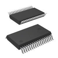
M37542F8FP Renesas Electronics America, M37542F8FP Datasheet - Page 60

M37542F8FP
Manufacturer Part Number
M37542F8FP
Description
IC 740 MCU FLASH 32K 36SSOP
Manufacturer
Renesas Electronics America
Series
740/38000r
Datasheet
1.M37542F8FPU0.pdf
(124 pages)
Specifications of M37542F8FP
Core Processor
740
Core Size
8-Bit
Speed
8MHz
Connectivity
SIO, UART/USART
Peripherals
POR, WDT
Number Of I /o
29
Program Memory Size
32KB (32K x 8)
Program Memory Type
FLASH
Ram Size
1K x 8
Voltage - Supply (vcc/vdd)
2.2 V ~ 5.5 V
Data Converters
A/D 8x10b
Oscillator Type
Internal
Operating Temperature
-20°C ~ 85°C
Package / Case
36-SSOP
Lead Free Status / RoHS Status
Contains lead / RoHS non-compliant
Eeprom Size
-
Available stocks
Company
Part Number
Manufacturer
Quantity
Price
Part Number:
M37542F8FP
Manufacturer:
MIT
Quantity:
20 000
Company:
Part Number:
M37542F8FP#U0
Manufacturer:
TI
Quantity:
109
7542 Group
Watchdog Timer
The watchdog timer gives a means for returning to a reset status
when the program fails to run on its normal loop due to a runaway.
The watchdog timer consists of an 8-bit watchdog timer H and an
8-bit watchdog timer L, being a 16-bit counter.
Standard operation of watchdog timer
The watchdog timer stops when the watchdog timer control regis-
ter (address 0039
value to the watchdog timer control register (address 0039
causes the watchdog timer to start to count down. When the
watchdog timer H underflows, an internal reset occurs. Accord-
ingly, it is programmed that the watchdog timer control register
(address 0039
When the watchdog timer control register (address 0039
read, the values of the high-order 6-bit of the watchdog timer H,
STP instruction function selection bit and watchdog timer H count
source selection bit are read.
Initial value of watchdog timer
By a reset or writing to the watchdog timer control register (ad-
dress 0039
watchdog timer L is set to “FF
Operation of watchdog timer H count source selection bit
A watchdog timer H count source can be selected by bit 7 of the
watchdog timer control register (address 0039
“0”, the count source becomes a watchdog timer L underflow sig-
nal. The detection time is 131.072 ms at f(X
When this bit is “1”, the count source becomes f(X
case, the detection time is 512 µs at f(X
This bit is cleared to “0” after reset.
Fig. 71 Block diagram of watchdog timer
Fig. 72 Structure of watchdog timer control register
Rev.3.03
REJ03B0006-0303
16
On-chip oscillator
Jul 11, 2008
), the watchdog timer H is set to “FF
Source clock selection
(auto-switch depending on setting of CPUM)
16
XIN clock
) can be set before an underflow occurs.
16
) is not set after reset. Writing an optional
STP Instruction function selection bit
b7
RESET
16
”.
Page 58 of 117
IN
Write “FF
watchdog timer
control register
)=8 MHz.
STP Instruction
IN
)=8 MHz.
16
1/16
). When this bit is
b0
16
IN
” to the
Watchdog timer control register
(WDTCON: address 0039
)/16. In this
16
Watchdog timer H (read only for high-order 6-bit)
STP instruction function selection bit
0 : System enters into the stop mode
1 : Internal reset occurs at the STP instruction execution
Watchdog timer H count source selection bit
0 : Watchdog timer L underflow
1 : f(X
” and the
Watchdog timer L (8)
at the STP instruction execution
16
IN
) is
16
)/16 or on-chip oscillator/16
)
Operation of STP instruction function selection bit
When “0” is set to STP instruction function selection bit, system
enters into the stop mode at the STP instruction execution.
When “1” is set to this bit, internal reset occurs at the STP instruc-
tion execution.
This bit is set to “1” by program, but it cannot be changed to “0” .
This bit is cleared to “0” after reset.
1. The watchdog timer is operating during the wait mode. Write data
2. The watchdog timer stops during the stop mode. However, the
3. The STP instruction function selection bit (bit 6 of watchdog
4. A count source of watchdog timer is affected by the clock divi-
to the watchdog timer control register to prevent timer underflow.
watchdog timer is running during the oscillation stabilizing time
after the STP instruction is released. In order to avoid the under-
flow of the watchdog timer, the watchdog timer control register
must be written just before executing the STP instruction.
timer control register (address 0039
once after releasing reset. After rewriting it is disable to write
any data to this bit.
sion selection bit of the CPU mode register.
The f(X
ing f(X
The on-chip oscillator output is supplied to the watchdog timer
when selecting the on-chip oscillator output as the CPU clock.
Notes on Watchdog Timer
“0”
16
“1”
Watchdog timer H count
source selection bit
, initial value: 3F
IN
IN
) as the CPU clock.
) clock is supplied to the watchdog timer when select-
Watchdog timer H (8)
Reset
circuit
16
)
Data bus
16
)) can be rewritten only
Internal
reset
Write "FF
watchdog timer
control register
16
" to the


