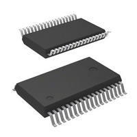
M37542F8FP Renesas Electronics America, M37542F8FP Datasheet - Page 104

M37542F8FP
Manufacturer Part Number
M37542F8FP
Description
IC 740 MCU FLASH 32K 36SSOP
Manufacturer
Renesas Electronics America
Series
740/38000r
Datasheet
1.M37542F8FPU0.pdf
(124 pages)
Specifications of M37542F8FP
Core Processor
740
Core Size
8-Bit
Speed
8MHz
Connectivity
SIO, UART/USART
Peripherals
POR, WDT
Number Of I /o
29
Program Memory Size
32KB (32K x 8)
Program Memory Type
FLASH
Ram Size
1K x 8
Voltage - Supply (vcc/vdd)
2.2 V ~ 5.5 V
Data Converters
A/D 8x10b
Oscillator Type
Internal
Operating Temperature
-20°C ~ 85°C
Package / Case
36-SSOP
Lead Free Status / RoHS Status
Contains lead / RoHS non-compliant
Eeprom Size
-
Available stocks
Company
Part Number
Manufacturer
Quantity
Price
Part Number:
M37542F8FP
Manufacturer:
MIT
Quantity:
20 000
Company:
Part Number:
M37542F8FP#U0
Manufacturer:
TI
Quantity:
109
7542 Group
Timing Requirements
Table 22 Timing requirements (1)
(FLASH ROM version: V
Notes 1: As for CAP
Table 23 Timing requirements (2)
(FLASH ROM version: V
Notes 1: As for CAP
Rev.3.03
REJ03B0006-0303
t
t
t
t
t
t
t
t
t
t
t
t
t
t
t
t
t
t
t
t
t
t
t
t
W
C
WH
WL
C
WH
WL
C
WH
WL
su
h
W
C
WH
WL
C
WH
WL
C
WH
WL
su
h
(S
(S
(X
(CNTR
(S
(X
(CNTR
(S
(RESET)
(RESET)
(RxD
(RxD
(X
(CNTR
(S
(X
(CNTR
(S
(X
(CNTR
(S
(X
(CNTR
(S
CLK1
CLK1
2: In this time, bit 6 of the serial I/O1 control register (address 001A
2: In this time, bit 6 of the serial I/O1 control register (address 001A
IN
CLK1
IN
CLK1
IN
CLK1
IN
CLK1
Symbol
Symbol
)
IN
CLK1
)
IN
CLK1
When bit 6 of the serial I/O1 control register is “0” (clock asynchronous serial I/O is selected), the rating values are divided by 4.
In this time, bit 6 of the serial I/O2 control register (address 0030
When bit 6 of the serial I/O2 control register is “0” (clock asynchronous serial I/O is selected), the rating values are divided by 4.
When bit 6 of the serial I/O1 control register is “0” (clock asynchronous serial I/O1 is selected), the rating values are divided by 4.
In this time, bit 6 of the serial I/O2 control register (address 0030
When bit 6 of the serial I/O2 control register is “0” (clock asynchronous serial I/O is selected), the rating values are divided by 4.
)
)
)
1
)
1
–RxD
–RxD
–S
–S
)
)
0
0
)
)
)
)
0
0
)
)
0
0
)
)
CLK1
CLK1
)
)
Jul 11, 2008
1
1
)
)
)
)
0
0
, CAP
, CAP
Reset input “L” pulse width
External clock input cycle time
External clock input “H” pulse width
External clock input “L” pulse width
CNTR
CNTR
CNTR
Serial I/O1, serial I/O2 clock input cycle time (Note 2)
Serial I/O1, serial I/O2 clock input “H” pulse width (Note 2)
Serial I/O1, serial I/O2 clock input “L” pulse width (Note 2)
Serial I/O1, serial I/O2 input set up time
Serial I/O1, serial I/O2 input hold time
1
1
, it is the value when noise filter is not used.
CC
, it is the value when noise filter is not used.
CC
= 4.0 to 5.5V, Mask ROM version: V
= 2.7 to 5.5V, Mask ROM version: V
0
0
0
0
0
0
, INT
, INT
, INT
, INT
input cycle time
input cycle time
Page 102 of 117
0
0
0
0
, INT
, INT
, INT
, INT
1
1
1
1
, CAP
, CAP
, CAP
, CAP
0
0
0
0
, CAP
, CAP
, CAP
, CAP
Parameter
Parameter
1
1
1
1
input “H” pulse width (Note 1)
input “L” pulse width (Note 1)
input “H” pulse width (Note 1)
input “L” pulse width (Note 1)
16
16
16
CC
16
CC
) is set to “1” (clock synchronous serial I/O is selected).
) is set to “1” (clock synchronous serial I/O is selected).
) is set to “1” (clock synchronous serial I/O is selected).
) is set to “1” (clock synchronous serial I/O is selected).
= 2.4 to 5.5 V, V
= 4.0 to 5.5 V, V
SS
SS
= 0 V, Ta = –20 to 85 °C, unless otherwise noted)
= 0 V, Ta = –20 to 85 °C, unless otherwise noted)
2000
125
200
800
370
370
220
100
250
100
100
500
230
230
950
950
400
200
Min.
Min.
50
50
80
80
2
2
Limits
Limits
Typ.
Typ.
Max.
Max.
Unit
Unit
µs
ns
ns
ns
ns
ns
ns
ns
ns
ns
ns
ns
µs
ns
ns
ns
ns
ns
ns
ns
ns
ns
ns
ns


