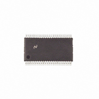
COP8SDE9IMT9/NOPB National Semiconductor, COP8SDE9IMT9/NOPB Datasheet - Page 24

COP8SDE9IMT9/NOPB
Manufacturer Part Number
COP8SDE9IMT9/NOPB
Description
IC MCU EEPROM 8BIT 8K 48-TSSOP
Manufacturer
National Semiconductor
Series
COP8™ 8Sr
Datasheet
1.COP8SDE9IMT9NOPB.pdf
(70 pages)
Specifications of COP8SDE9IMT9/NOPB
Core Processor
COP8
Core Size
8-Bit
Speed
20MHz
Connectivity
Microwire/Plus (SPI), UART/USART
Peripherals
POR, PWM, WDT
Number Of I /o
39
Program Memory Size
8KB (8K x 8)
Program Memory Type
FLASH
Ram Size
256 x 8
Voltage - Supply (vcc/vdd)
2.7 V ~ 5.5 V
Oscillator Type
Internal
Operating Temperature
0°C ~ 70°C
Package / Case
48-TSSOP
Lead Free Status / RoHS Status
Lead free / RoHS Compliant
Eeprom Size
-
Data Converters
-
Other names
*COP8SDE9IMT9
*COP8SDE9IMT9/NOPB
COP8SDE9IMT9
*COP8SDE9IMT9/NOPB
COP8SDE9IMT9
www.national.com
PGMTIM_SET
PAGE_ERASE
5.0 In-System Programming
memory and reprogram it. If the device is subsequently reset
before the Flex bit has been erased by specific Page Erase
or Mass Erase ISP commands, execution will start from
location 0000 in the Flash program memory. The high volt-
age (2 x V
Security bit in the Option Register. The Security bit, if set,
can only be erased by a Mass Erase of the entire contents of
the Flash Memory unless under the control of User ISP
routines in the Application Program.
While the G6 pin is at high voltage, the Load Clock will be
output onto G5, which will look like an SK clock to the
MICROWIRE/PLUS routine executing in slave mode. How-
ever, when G6 is at high voltage, the G6 input will also look
like a logic 1. The MICROWIRE/PLUS routine in Boot ROM
monitors the G6 input, waits for it to go low, debounces it,
and then enables the ISP routine. CAUTION: The Load clock
on G5 could be in conflict with the user’s external SK. It is up
to the user to resolve this conflict, as this condition is con-
sidered a minor issue that’s only encountered during soft-
ware development. The user should also be cautious of
the high voltage applied to the G6 pin. This high voltage
could damage other circuitry connected to the G6 pin
(e.g. the parallel port of a PC). The user may wish to
disconnect other circuitry while G6 is connected to the high
voltage.
V
to G6.
The correct sequence to be used to force execution from
Boot ROM is :
1. Disconnect G6 from the source of data for MICROWIRE/
2. Apply V
3. Pull RESET Low.
4. After V
5. Pull RESET High.
6. After a delay of at least three instruction cycles, remove
(Continued)
CC
PLUS ISP.
2 x V
time of the high voltage on G6 is slower than the mini-
mum in the Electrical Specifications. Figure 14 shows a
possible circuit dliagram for implementing the 2 x V
Be aware of the typical input current on the G6 pin when
the high voltage is applied. The resistor used in the RC
network, and the high voltage used, should be chosen to
keep the high voltage at the G6 pin between 2 x V
V
the high voltage from G6.
must be valid and stable before high voltage is applied
Command
CC
+7V.
CC
CC
CC
CC
and V
) on G6 will not erase either the Flex or the
is valid and stable, connect a voltage between
to the device.
CC
+7V to the G6 pin. Ensure that the rise
Write Pulse Timing
Register
Page Erase
Function
TABLE 11. MICROWIRE/PLUS ISP Commands
CC
and
CC
Value (Hex)
Command
.
0x3B
0xB3
24
5.6 RETURN TO FLASH MEMORY WITHOUT
HARDWARE RESET
After programming the entire program memory, including
options, it is necessary to exit the Boot ROM and return to
the flash program memory for program execution. Upon
receipt and completion of the EXIT command through the
MICROWIRE/PLUS ISP, the ISP code will reset the part and
begin execution from the flash program memory as de-
scribed in the Reset section. This assumes that the FLEX bit
in the Option register was programmed to 1.
5.7 MICROWIRE/PLUS ISP
National Semiconductor provides a program, which is avail-
able from our web site at www.national.com/cop8, that is
capable of programming a device from the parallel port of a
PC. The software accepts manually input commands and is
capable of downloading standard Intel HEX Format files.
Users who wish to write their own MICROWIRE/PLUS ISP
host software should refer to the COP8 FLASH ISP User
Manual, available from the same web site. This document
includes details of command format and delays necessary
between command bytes.
The MICROWIRE/PLUS ISP supports the following features
and commands:
• Write a value to the ISP Write Timing Register. NOTE:
• Erase the entire flash program memory (mass erase).
• Erase a page at a specified address.
• Read Option register.
• Read a byte from a specified address.
• Write a byte to a specified address.
• Read multiple bytes starting at a specified address.
• Write multiple bytes starting at a specified address.
• Exit ISP and return execution to flash program memory.
The following table lists the MICROWIRE/PLUS ISP com-
mands and provides information on required parameters and
return values.
FIGURE 14. Circuit Diagram for Implementing the 2 x
This must be the first command after entering
MICROWIRE/PLUS ISP mode.
Value
Starting Address of
Page
Parameters
V
CC
N/A
N/A
Return Data
20032766


