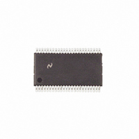
COP8SDE9IMT9/NOPB National Semiconductor, COP8SDE9IMT9/NOPB Datasheet - Page 16

COP8SDE9IMT9/NOPB
Manufacturer Part Number
COP8SDE9IMT9/NOPB
Description
IC MCU EEPROM 8BIT 8K 48-TSSOP
Manufacturer
National Semiconductor
Series
COP8™ 8Sr
Datasheet
1.COP8SDE9IMT9NOPB.pdf
(70 pages)
Specifications of COP8SDE9IMT9/NOPB
Core Processor
COP8
Core Size
8-Bit
Speed
20MHz
Connectivity
Microwire/Plus (SPI), UART/USART
Peripherals
POR, PWM, WDT
Number Of I /o
39
Program Memory Size
8KB (8K x 8)
Program Memory Type
FLASH
Ram Size
256 x 8
Voltage - Supply (vcc/vdd)
2.7 V ~ 5.5 V
Oscillator Type
Internal
Operating Temperature
0°C ~ 70°C
Package / Case
48-TSSOP
Lead Free Status / RoHS Status
Lead free / RoHS Compliant
Eeprom Size
-
Data Converters
-
Other names
*COP8SDE9IMT9
*COP8SDE9IMT9/NOPB
COP8SDE9IMT9
*COP8SDE9IMT9/NOPB
COP8SDE9IMT9
www.national.com
4.0 Functional Description
segment (containing the 16 memory registers, I/O registers,
control registers, etc.) is always available regardless of the
contents of the S register, since the upper base segment
(address range 0080 to 00FF) is independent of data seg-
ment extension.
The instructions that utilize the stack pointer (SP) always
reference the stack as part of the base segment (Segment
0), regardless of the contents of the S register. The S register
is not changed by these instructions. Consequently, the
stack (used with subroutine linkage and interrupts) is always
located in the base segment. The stack pointer will be initial-
ized to point at data memory location 006F as a result of
reset.
4.4.1 Virtual EEPROM
The Flash memory and the User ISP functions (see Section
5.7), provide the user with the capability to use the flash
program memory to back up user defined sections of RAM.
This effectively provides the user with the same nonvolatile
data storage as EEPROM. Management, and even the
amount of memory used, are the responsibility of the user,
however the flash memory read and write functions have
been provided in the boot ROM.
One typical method of using the Virtual EEPROM feature
would be for the user to copy the data to RAM during system
initialization, periodically, and if necessary, erase the page of
Flash and copy the contents of the RAM back to the Flash.
4.5 OPTION REGISTER
The Option register, located at address 0x3FFF (hex) in the
Flash Program Memory, is used to configure the user select-
able security, WATCHDOG, and HALT options. The register
can be programmed only in external Flash Memory program-
ming or ISP Programming modes. Therefore, the register
(Continued)
FIGURE 7. RAM Organization
16
The 128 bytes of RAM contained in the base segment are
split between the lower and upper base segments. The first
112 bytes of RAM are resident from address 0000 to 006F in
the lower base segment, while the remaining 16 bytes of
RAM represent the 16 data memory registers located at
addresses 00F0 to 00FF of the upper base segment. No
RAM is located at the upper sixteen addresses (0070 to
007F) of the lower base segment.
Additional RAM beyond these initial 128 bytes, however, will
always be memory mapped in groups of 128 bytes (or less)
at the data segment address extensions (XX00 to XX7F) of
the lower base segment. The additional 128 bytes of RAM in
this device are memory mapped at address locations 0100
through 017F.
must be programmed at the same time as the program
memory. The contents of the Option register shipped from
the factory read 00 Hex.
The format of the Option register is as follows:
Bits 7, 6 These bits are reserved and must be 0.
Bit 5
Bits 4, 3 These bits are reserved and must be 0.
Bit 2
Bit 7
= 1
= 0
= 1
Reserved
Bit 6
Security enabled. Flash Memory read and write
are not allowed except in User ISP/Virtual E
mands. Mass Erase is allowed.
Security disabled. Flash Memory read and write
are allowed.
WATCHDOG feature disabled. G1 is a general
purpose I/O.
SECURITY
Bit 5
Bit 4
Reserved
Bit 3
WATCH
Bit 2
DOG
20032710
HALT
Bit 1
2
FLEX
Bit 0
com-


