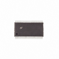
COP8SDE9IMT9/NOPB National Semiconductor, COP8SDE9IMT9/NOPB Datasheet - Page 14

COP8SDE9IMT9/NOPB
Manufacturer Part Number
COP8SDE9IMT9/NOPB
Description
IC MCU EEPROM 8BIT 8K 48-TSSOP
Manufacturer
National Semiconductor
Series
COP8™ 8Sr
Datasheet
1.COP8SDE9IMT9NOPB.pdf
(70 pages)
Specifications of COP8SDE9IMT9/NOPB
Core Processor
COP8
Core Size
8-Bit
Speed
20MHz
Connectivity
Microwire/Plus (SPI), UART/USART
Peripherals
POR, PWM, WDT
Number Of I /o
39
Program Memory Size
8KB (8K x 8)
Program Memory Type
FLASH
Ram Size
256 x 8
Voltage - Supply (vcc/vdd)
2.7 V ~ 5.5 V
Oscillator Type
Internal
Operating Temperature
0°C ~ 70°C
Package / Case
48-TSSOP
Lead Free Status / RoHS Status
Lead free / RoHS Compliant
Eeprom Size
-
Data Converters
-
Other names
*COP8SDE9IMT9
*COP8SDE9IMT9/NOPB
COP8SDE9IMT9
*COP8SDE9IMT9/NOPB
COP8SDE9IMT9
www.national.com
3.0 Pin Descriptions
L7 Multi-Input Wake-up
L6 Multi-Input Wake-up
L5 Multi-Input Wake-up or T2B (Timer T2B Input)
L4 Multi-input Wake-up or T2A (Timer T2A Input)
L3 Multi-Input Wake-up and/or RDX (USART Receive)
L2 Multi-Input Wake-up or TDX (USART Transmit)
L1 Multi-Input Wake-up and/or CKX (USART Clock) (Low
L0 Multi-Input Wake-up (Low Speed Oscillator Input)
FIGURE 4. I/O Port Configurations — Output Mode
Speed Oscillator Output)
FIGURE 3. I/O Port Configurations
(Continued)
20032761
20032760
14
3.1 EMULATION CONNECTION
Connection to the emulation system is made via a 2 x 7
connector which interrupts the continuity of the RESET, G0,
G1, G2 and G3 signals between the COP8 device and the
rest of the target system (as shown in Figure 6 ). This con-
nector can be designed into the production pc board and can
be replaced by jumpers or signal traces when emulation is
no longer necessary. The emulator will replicate all functions
of G0 - G3 and RESET. For proper operation, no connection
should be made on the device side of the emulator connec-
tor.
4.0 Functional Description
The architecture of the device is a modified Harvard archi-
tecture. With the Harvard architecture, the program memory
(Flash) is separate from the data store memory (RAM). Both
Program Memory and Data Memory have their own separate
addressing space with separate address buses. The archi-
tecture, though based on the Harvard architecture, permits
transfer of data from Flash Memory to RAM.
FIGURE 5. I/O Port Configurations — Input Mode
FIGURE 6. Emulation Connection
20032709
20032762


