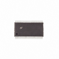
COP8SDE9IMT9/NOPB National Semiconductor, COP8SDE9IMT9/NOPB Datasheet - Page 19

COP8SDE9IMT9/NOPB
Manufacturer Part Number
COP8SDE9IMT9/NOPB
Description
IC MCU EEPROM 8BIT 8K 48-TSSOP
Manufacturer
National Semiconductor
Series
COP8™ 8Sr
Datasheet
1.COP8SDE9IMT9NOPB.pdf
(70 pages)
Specifications of COP8SDE9IMT9/NOPB
Core Processor
COP8
Core Size
8-Bit
Speed
20MHz
Connectivity
Microwire/Plus (SPI), UART/USART
Peripherals
POR, PWM, WDT
Number Of I /o
39
Program Memory Size
8KB (8K x 8)
Program Memory Type
FLASH
Ram Size
256 x 8
Voltage - Supply (vcc/vdd)
2.7 V ~ 5.5 V
Oscillator Type
Internal
Operating Temperature
0°C ~ 70°C
Package / Case
48-TSSOP
Lead Free Status / RoHS Status
Lead free / RoHS Compliant
Eeprom Size
-
Data Converters
-
Other names
*COP8SDE9IMT9
*COP8SDE9IMT9/NOPB
COP8SDE9IMT9
*COP8SDE9IMT9/NOPB
COP8SDE9IMT9
4.0 Functional Description
Timer starts counting the 240 to 256 t
soon as the V
mately 1.8V). This behavior is shown in Figure 10 .
In Case 1, V
undefined until the supply is greater than approximately
1.0V. At this time the brownout circuit becomes active and
holds the device in RESET. As the supply passes a level of
about 1.8V, a delay of about 3 ms (t
Timer is preset to a value between 00F0 and 00FF (hex).
Once V
Timer is allowed to count down (t
Case 2 shows a subsequent dip in the supply voltage which
goes below the approximate 1.8V level. As V
V
back above the 1.8V level, t
supply rise time is longer for this case, t
V
greater than V
Case 3 shows a dip in the supply where V
V
V
goes back above V
If the Brownout Reset feature is enabled, the internal reset
will not be turned off until the Idle Timer underflows. The
internal reset will perform the same functions as external
reset. The device is guaranteed to operate at the specified
frequency down to the specified brownout voltage. After the
underflow, the logic is designed such that no additional
internal resets occur as long as V
brownout voltage.
The device is relatively immune to short duration negative-
going V
filtering of V
works correctly. Power supply decoupling is vital even in
battery powered systems.
There are two optional brownout voltages. The part numbers
for the three versions of this device are:
Refer to the device specifications for the actual V
ages.
High brownout voltage devices are guaranteed to operate at
10MHz down to the high brownout voltage. Low brownout
voltage devices are guaranteed to operate at 3.33MHz down
to the low brownout voltage. Low brownout voltage de-
vices are not guaranteed to operate at 10MHz down to
the low brownout voltage.
bor
CC
bor
CC
COP8SBE, V
COP8SCE, V
COP8SDE, BOR is disabled.
, the internal RESET signal is asserted. When V
, but not below 1.8V. On-chip RESET is asserted when
rises above V
goes below V
CC
CC
is greater than V
transients (glitches). It is essential that good
CC
CC
bor
CC
be done to ensure that the brownout feature
bor
bor
.
rises from 0V and the on-chip RESET is
rises above the trigger voltage (approxi-
bor
bor
= low voltage range
= high voltage range
bor
and t
.
and t
id
id
bor
starts immediately when V
d
starts as soon as the supply
is started. Since the power
and t
id
).
d
CC
) is started and the Idle
d
C
has expired, the Idle
. This delay starts as
d
remains above the
has expired before
CC
CC
(Continued)
drops below
drops below
CC
bor
rises
CC
volt-
is
19
Under no circumstances should the RESET pin be allowed
to float. If the on-chip Brownout Reset feature is being used,
the RESET pin should be connected directly to V
RESET input may also be connected to an external pull-up
resistor or to other external circuitry. The output of the brown-
out reset detector will always preset the Idle Timer to a value
between 00F0 and 00FF (240 to 256 t
internal reset will be generated.
If the BOR feature is disabled, then no internal resets are
generated and the Idle Timer will power-up with an unknown
value. In this case, the external RESET must be used. When
BOR is disabled, this on-chip circuitry is disabled and draws
no DC current.
The contents of data registers and RAM are unknown fol-
lowing the on-chip reset.
4.8 OSCILLATOR CIRCUITS
The device has two crystal oscillators to facilitate low power
operation while maintaining throughput when required. Fur-
ther information on the use of the two oscillators is found in
Section 7.0 Power Saving Features. The low speed oscillator
utilizes the L0 and L1 port pins. References in the following
text to CKI will also apply to L0 and references to G7/CKO
will also apply to L1.
4.8.1 Oscillator
CKI is the clock input while G7/CKO is the clock generator
output to the crystal. An on-chip bias resistor connected
between CKI and CKO is provided to reduce system part
count. The value of the resistor is in the range of 0.5M to 2M
(typically 1.0M). Table 3 shows the component values re-
quired for various standard crystal values. Resistor R2 is
on-chip, for the high speed oscillator, and is shown for
reference. Figure 12 shows the crystal oscillator connection
diagram. A ceramic resonator of the required frequency may
be used in place of a crystal if the accuracy requirements are
not quite as strict.
FIGURE 11. Reset Circuit Using Power-On Reset
C
). At this time, the
20032714
www.national.com
CC
. The


