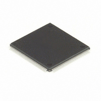
MC68HC16Z1CPV25 Freescale Semiconductor, MC68HC16Z1CPV25 Datasheet - Page 400

MC68HC16Z1CPV25
Manufacturer Part Number
MC68HC16Z1CPV25
Description
IC MPU 1K RAM 25MHZ 144-LQFP
Manufacturer
Freescale Semiconductor
Series
HC16r
Datasheet
1.MC68HC16Z1VEH16.pdf
(500 pages)
Specifications of MC68HC16Z1CPV25
Core Processor
CPU16
Core Size
16-Bit
Speed
25MHz
Connectivity
EBI/EMI, SCI, SPI
Peripherals
POR, PWM, WDT
Number Of I /o
16
Program Memory Type
ROMless
Ram Size
1K x 8
Voltage - Supply (vcc/vdd)
2.7 V ~ 5.5 V
Data Converters
A/D 8x10b
Oscillator Type
Internal
Operating Temperature
-40°C ~ 85°C
Package / Case
144-LQFP
Lead Free Status / RoHS Status
Contains lead / RoHS non-compliant
Eeprom Size
-
Program Memory Size
-
Other names
Q1141110
Available stocks
Company
Part Number
Manufacturer
Quantity
Price
Company:
Part Number:
MC68HC16Z1CPV25
Manufacturer:
MOT
Quantity:
5 510
Company:
Part Number:
MC68HC16Z1CPV25
Manufacturer:
SIEMENS
Quantity:
5 510
Company:
Part Number:
MC68HC16Z1CPV25
Manufacturer:
FREESCAL
Quantity:
624
Company:
Part Number:
MC68HC16Z1CPV25
Manufacturer:
Freescale Semiconductor
Quantity:
10 000
- Current page: 400 of 500
- Download datasheet (6Mb)
BOOT — Boot ROM Control
LOCK — Lock Registers
EMUL — Emulation Mode Control
ASPC[1:0] — ROM Array Space
WAIT[1:0] — Wait States Field
D-26
Reset state of BOOT is specified at mask time. This is a read-only bit.
Bootstrap operation is overridden if STOP = 1 at reset.
The reset state of LOCK is specified at mask time. If the reset state of the LOCK is
zero, it can be set once after reset to allow protection of the registers after initialization.
Once the LOCK bit is set, it cannot be cleared again until after a reset. LOCK protects
the ASPC and WAIT fields, as well as the ROMBAL and ROMBAH registers. ASPC,
ROMBAL and ROMBAH are also protected by the STOP bit.
Because the MC68HC16Z2 and the MC68HC16Z3 do not support ROM emulation
mode, this bit should never be set.
The ASPC field limits access to the SRAM array in microcontrollers that support sep-
arate user and supervisor operating modes. ASPC1 has no effect because the CPU16
operates in supervisor mode only. This bit may be read or written at any time. The
reset state of ASPC[1:0] is specified at mask time.
coding.
WAIT[1:0] specifies the number of wait states inserted by the MRM during ROM array
accesses. The reset state of WAIT[1:0] is user specified. The field can be written only
if LOCK = 0 and STOP = 1.
0 = ROM responds to bootstrap word locations during reset vector fetch.
1 = ROM does not respond to bootstrap word locations during reset vector fetch.
0 = Write lock disabled. Protected registers and fields can be written.
1 = Write lock enabled. Protected registers and fields cannot be written.
0 = Normal ROM operation
1 = Accesses to the ROM array are forced external, allowing memory selected by
the CSM pin to respond to the access.
WAIT[1:0]
00
01
10
11
Freescale Semiconductor, Inc.
For More Information On This Product,
Table D-22 ROM Array Space Field
ASPC[1:0]
Table D-23 Wait States Field
X0
X1
Table D-23
Go to: www.freescale.com
Wait States
Number of
REGISTER SUMMARY
–1
0
1
2
Program and data accesses
Program access only
shows the wait states field.
State Specified
Clocks per Transfer
Table D-22
3
4
5
2
shows ASPC[1:0] en-
M68HC16 Z SERIES
USER’S MANUAL
Related parts for MC68HC16Z1CPV25
Image
Part Number
Description
Manufacturer
Datasheet
Request
R
Part Number:
Description:
Manufacturer:
Freescale Semiconductor, Inc
Datasheet:
Part Number:
Description:
Manufacturer:
Freescale Semiconductor, Inc
Datasheet:
Part Number:
Description:
Manufacturer:
Freescale Semiconductor, Inc
Datasheet:
Part Number:
Description:
Manufacturer:
Freescale Semiconductor, Inc
Datasheet:
Part Number:
Description:
Manufacturer:
Freescale Semiconductor, Inc
Datasheet:
Part Number:
Description:
Manufacturer:
Freescale Semiconductor, Inc
Datasheet:
Part Number:
Description:
Manufacturer:
Freescale Semiconductor, Inc
Datasheet:
Part Number:
Description:
Manufacturer:
Freescale Semiconductor, Inc
Datasheet:
Part Number:
Description:
Manufacturer:
Freescale Semiconductor, Inc
Datasheet:
Part Number:
Description:
Manufacturer:
Freescale Semiconductor, Inc
Datasheet:
Part Number:
Description:
Manufacturer:
Freescale Semiconductor, Inc
Datasheet:
Part Number:
Description:
Manufacturer:
Freescale Semiconductor, Inc
Datasheet:
Part Number:
Description:
Manufacturer:
Freescale Semiconductor, Inc
Datasheet:
Part Number:
Description:
Manufacturer:
Freescale Semiconductor, Inc
Datasheet:
Part Number:
Description:
Manufacturer:
Freescale Semiconductor, Inc
Datasheet:


