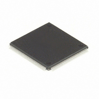
MC68HC16Z1CPV25 Freescale Semiconductor, MC68HC16Z1CPV25 Datasheet - Page 184

MC68HC16Z1CPV25
Manufacturer Part Number
MC68HC16Z1CPV25
Description
IC MPU 1K RAM 25MHZ 144-LQFP
Manufacturer
Freescale Semiconductor
Series
HC16r
Datasheet
1.MC68HC16Z1VEH16.pdf
(500 pages)
Specifications of MC68HC16Z1CPV25
Core Processor
CPU16
Core Size
16-Bit
Speed
25MHz
Connectivity
EBI/EMI, SCI, SPI
Peripherals
POR, PWM, WDT
Number Of I /o
16
Program Memory Type
ROMless
Ram Size
1K x 8
Voltage - Supply (vcc/vdd)
2.7 V ~ 5.5 V
Data Converters
A/D 8x10b
Oscillator Type
Internal
Operating Temperature
-40°C ~ 85°C
Package / Case
144-LQFP
Lead Free Status / RoHS Status
Contains lead / RoHS non-compliant
Eeprom Size
-
Program Memory Size
-
Other names
Q1141110
Available stocks
Company
Part Number
Manufacturer
Quantity
Price
Company:
Part Number:
MC68HC16Z1CPV25
Manufacturer:
MOT
Quantity:
5 510
Company:
Part Number:
MC68HC16Z1CPV25
Manufacturer:
SIEMENS
Quantity:
5 510
Company:
Part Number:
MC68HC16Z1CPV25
Manufacturer:
FREESCAL
Quantity:
624
Company:
Part Number:
MC68HC16Z1CPV25
Manufacturer:
Freescale Semiconductor
Quantity:
10 000
- Current page: 184 of 500
- Download datasheet (6Mb)
7.3 MRM Array Address Space Type
7.4 Normal Access
7-2
The MRM array can be mapped to any 8-Kbyte boundary in the memory map, but must
not overlap other module control registers (overlap makes the registers inaccessible).
If the array overlaps the MRM register block, addresses in the register block are ac-
cessed instead of the corresponding ROM array addresses.
ROMBAH and ROMBAL can only be written while the ROM is in low-power stop mode
(MRMCR STOP = 1) and the base address lock (MRMCR LOCK = 0) is disabled.
LOCK can be written once only to a value of one; subsequent writes are ignored. This
prevents accidental remapping of the array.
ASPC[1:0] in MRMCR determines ROM array address space type. The module can
respond to both program and data space accesses or to program space accesses
only. The default value of ASPC[1:0] is established during mask programming, but the
value can be changed after reset if the LOCK bit in the MRMCR has not been masked
to a value of one. Because the CPU16 operates in supervisor mode only, ASPC1 has
no effect.
Table 7-1
Refer to
types and program/data space access. Refer to
formation on addressing modes.
The array can be accessed by byte, word, or long word. A byte or aligned word access
takes a minimum of one bus cycle (two system clocks). A long word or misaligned
word access requires a minimum of two bus cycles.
Access time can be optimized for a particular application by inserting wait states into
each access. The number of wait states inserted is determined by the value of
WAIT[1:0] in the MRMCR. Two, three, four, or five clock accesses can be specified.
The default value WAIT[1:0] is established during mask programming, but field value
can be changed after reset if the LOCK bit in the MRMCR has not been masked to a
value of one.
Table 7-2
5.5.1.7 Function Codes
shows ASPC[1:0] field encodings.
shows WAIT[1:0] field encodings.
Freescale Semiconductor, Inc.
For More Information On This Product,
Table 7-1 ROM Array Space Field
ASPC[1:0]
X0
X1
Go to: www.freescale.com
MASKED ROM MODULE
for more information concerning address space
Program and data accesses
Program access only
State Specified
4.6 Addressing Modes
M68HC16 Z SERIES
USER’S MANUAL
for more in-
Related parts for MC68HC16Z1CPV25
Image
Part Number
Description
Manufacturer
Datasheet
Request
R
Part Number:
Description:
Manufacturer:
Freescale Semiconductor, Inc
Datasheet:
Part Number:
Description:
Manufacturer:
Freescale Semiconductor, Inc
Datasheet:
Part Number:
Description:
Manufacturer:
Freescale Semiconductor, Inc
Datasheet:
Part Number:
Description:
Manufacturer:
Freescale Semiconductor, Inc
Datasheet:
Part Number:
Description:
Manufacturer:
Freescale Semiconductor, Inc
Datasheet:
Part Number:
Description:
Manufacturer:
Freescale Semiconductor, Inc
Datasheet:
Part Number:
Description:
Manufacturer:
Freescale Semiconductor, Inc
Datasheet:
Part Number:
Description:
Manufacturer:
Freescale Semiconductor, Inc
Datasheet:
Part Number:
Description:
Manufacturer:
Freescale Semiconductor, Inc
Datasheet:
Part Number:
Description:
Manufacturer:
Freescale Semiconductor, Inc
Datasheet:
Part Number:
Description:
Manufacturer:
Freescale Semiconductor, Inc
Datasheet:
Part Number:
Description:
Manufacturer:
Freescale Semiconductor, Inc
Datasheet:
Part Number:
Description:
Manufacturer:
Freescale Semiconductor, Inc
Datasheet:
Part Number:
Description:
Manufacturer:
Freescale Semiconductor, Inc
Datasheet:
Part Number:
Description:
Manufacturer:
Freescale Semiconductor, Inc
Datasheet:


