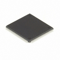
MC68HC16Z1CPV25 Freescale Semiconductor, MC68HC16Z1CPV25 Datasheet - Page 192

MC68HC16Z1CPV25
Manufacturer Part Number
MC68HC16Z1CPV25
Description
IC MPU 1K RAM 25MHZ 144-LQFP
Manufacturer
Freescale Semiconductor
Series
HC16r
Datasheet
1.MC68HC16Z1VEH16.pdf
(500 pages)
Specifications of MC68HC16Z1CPV25
Core Processor
CPU16
Core Size
16-Bit
Speed
25MHz
Connectivity
EBI/EMI, SCI, SPI
Peripherals
POR, PWM, WDT
Number Of I /o
16
Program Memory Type
ROMless
Ram Size
1K x 8
Voltage - Supply (vcc/vdd)
2.7 V ~ 5.5 V
Data Converters
A/D 8x10b
Oscillator Type
Internal
Operating Temperature
-40°C ~ 85°C
Package / Case
144-LQFP
Lead Free Status / RoHS Status
Contains lead / RoHS non-compliant
Eeprom Size
-
Program Memory Size
-
Other names
Q1141110
Available stocks
Company
Part Number
Manufacturer
Quantity
Price
Company:
Part Number:
MC68HC16Z1CPV25
Manufacturer:
MOT
Quantity:
5 510
Company:
Part Number:
MC68HC16Z1CPV25
Manufacturer:
SIEMENS
Quantity:
5 510
Company:
Part Number:
MC68HC16Z1CPV25
Manufacturer:
FREESCAL
Quantity:
624
Company:
Part Number:
MC68HC16Z1CPV25
Manufacturer:
Freescale Semiconductor
Quantity:
10 000
- Current page: 192 of 500
- Download datasheet (6Mb)
8.6.4 Comparator
8.7 Digital Control Subsystem
8.7.1 Control/Status Registers
8.7.2 Clock and Prescaler Control
8-6
The comparator indicates whether each approximation output from the RC DAC array
during resolution is higher or lower than the sampled input voltage. Comparator output
is fed to the digital control logic, which sets or clears each bit in the successive approx-
imation register in sequence, MSB first.
The digital control subsystem includes control and status registers, clock and prescal-
er control logic, channel and reference select logic, conversion sequence control logic,
and the successive approximation register.
The subsystem controls the multiplexer and the output of the RC array during sample
and conversion periods, stores the results of comparison in the successive-approxi-
mation register, then transfers results to the result registers.
There are two control registers (ADCTL0, ADCTL1) and one status register
(ADCSTAT). ADCTL0 controls conversion resolution, sample time, and clock/prescal-
er value. ADCTL1 controls analog input selection, conversion mode, and initiation of
conversion. A write to ADCTL0 aborts the current conversion sequence and halts the
ADC. Conversion must be restarted by writing to ADCTL1. A write to ADCTL1 aborts
the current conversion sequence and starts a new sequence with parameters altered
by the write. ADCSTAT shows conversion sequence status, conversion channel sta-
tus, and conversion completion status.
The following paragraphs are a general discussion of control function.
Digital Converter Module
and fields.
The ADC clock is derived from the system clock by a programmable prescaler. ADC
clock period is determined by the value of the PRS field in ADCTL0. The prescaler has
two stages. The first stage is a 5-bit modulus counter. It divides the system clock by
any value from two to 32 (PRS[4:0] = %00000 to %11111). The second stage is a di-
vide-by-two circuit.
Table 8-3
Freescale Semiconductor, Inc.
For More Information On This Product,
ANALOG-TO-DIGITAL CONVERTER
shows the ADC address map and discusses register bits
Go to: www.freescale.com
shows prescaler output values.
M68HC16 Z SERIES
D.5 Analog-to-
USER’S MANUAL
Related parts for MC68HC16Z1CPV25
Image
Part Number
Description
Manufacturer
Datasheet
Request
R
Part Number:
Description:
Manufacturer:
Freescale Semiconductor, Inc
Datasheet:
Part Number:
Description:
Manufacturer:
Freescale Semiconductor, Inc
Datasheet:
Part Number:
Description:
Manufacturer:
Freescale Semiconductor, Inc
Datasheet:
Part Number:
Description:
Manufacturer:
Freescale Semiconductor, Inc
Datasheet:
Part Number:
Description:
Manufacturer:
Freescale Semiconductor, Inc
Datasheet:
Part Number:
Description:
Manufacturer:
Freescale Semiconductor, Inc
Datasheet:
Part Number:
Description:
Manufacturer:
Freescale Semiconductor, Inc
Datasheet:
Part Number:
Description:
Manufacturer:
Freescale Semiconductor, Inc
Datasheet:
Part Number:
Description:
Manufacturer:
Freescale Semiconductor, Inc
Datasheet:
Part Number:
Description:
Manufacturer:
Freescale Semiconductor, Inc
Datasheet:
Part Number:
Description:
Manufacturer:
Freescale Semiconductor, Inc
Datasheet:
Part Number:
Description:
Manufacturer:
Freescale Semiconductor, Inc
Datasheet:
Part Number:
Description:
Manufacturer:
Freescale Semiconductor, Inc
Datasheet:
Part Number:
Description:
Manufacturer:
Freescale Semiconductor, Inc
Datasheet:
Part Number:
Description:
Manufacturer:
Freescale Semiconductor, Inc
Datasheet:


