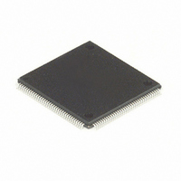
MC68HC16Z1CPV25 Freescale Semiconductor, MC68HC16Z1CPV25 Datasheet - Page 240

MC68HC16Z1CPV25
Manufacturer Part Number
MC68HC16Z1CPV25
Description
IC MPU 1K RAM 25MHZ 144-LQFP
Manufacturer
Freescale Semiconductor
Series
HC16r
Datasheet
1.MC68HC16Z1VEH16.pdf
(500 pages)
Specifications of MC68HC16Z1CPV25
Core Processor
CPU16
Core Size
16-Bit
Speed
25MHz
Connectivity
EBI/EMI, SCI, SPI
Peripherals
POR, PWM, WDT
Number Of I /o
16
Program Memory Type
ROMless
Ram Size
1K x 8
Voltage - Supply (vcc/vdd)
2.7 V ~ 5.5 V
Data Converters
A/D 8x10b
Oscillator Type
Internal
Operating Temperature
-40°C ~ 85°C
Package / Case
144-LQFP
Lead Free Status / RoHS Status
Contains lead / RoHS non-compliant
Eeprom Size
-
Program Memory Size
-
Other names
Q1141110
Available stocks
Company
Part Number
Manufacturer
Quantity
Price
Company:
Part Number:
MC68HC16Z1CPV25
Manufacturer:
MOT
Quantity:
5 510
Company:
Part Number:
MC68HC16Z1CPV25
Manufacturer:
SIEMENS
Quantity:
5 510
Company:
Part Number:
MC68HC16Z1CPV25
Manufacturer:
FREESCAL
Quantity:
624
Company:
Part Number:
MC68HC16Z1CPV25
Manufacturer:
Freescale Semiconductor
Quantity:
10 000
- Current page: 240 of 500
- Download datasheet (6Mb)
9.4.3.9 Internal Loop Mode
9-30
A receiver is placed in wake-up mode by setting the RWU bit in SCCR1. While RWU
is set, receiver status flags and interrupts are disabled. Although the CPU16 can clear
RWU, it is normally cleared by hardware during wake-up.
The WAKE bit in SCCR1 determines which type of wake-up is used. When WAKE =
0, idle-line wake-up is selected. When WAKE = 1, address-mark wake-up is selected.
Both types require a software-based device addressing and recognition scheme.
Idle-line wake-up allows a receiver to sleep until an idle line is detected. When an idle-
line is detected, the receiver clears RWU and wakes up. The receiver waits for the first
frame of the next transmission. The byte is received normally, transferred to RDR, and
the RDRF flag is set. If software does not recognize the address, it can set RWU and
put the receiver back to sleep. For idle-line wake-up to work, there must be a minimum
of one frame of idle line between transmissions. There must be no idle time between
frames within a transmission.
Address-mark wake-up uses a special frame format to wake up the receiver. When the
MSB of an address-mark frame is set, that frame contains address information. The
first frame of each transmission must be an address frame. When the MSB of a frame
is set, the receiver clears RWU and wakes up. The byte is received normally, trans-
ferred to the RDR, and the RDRF flag is set. If software does not recognize the ad-
dress, it can set RWU and put the receiver back to sleep. Address-mark wake-up
allows idle time between frames and eliminates idle time between transmissions. How-
ever, there is a loss of efficiency because of an additional bit-time per frame.
The LOOPS bit in SCCR1 controls a feedback path in the data serial shifter. When
LOOPS is set, the SCI transmitter output is fed back into the receive serial shifter. TXD
is asserted (idle line). Both transmitter and receiver must be enabled before entering
loop mode.
Freescale Semiconductor, Inc.
For More Information On This Product,
QUEUED SERIAL MODULE
Go to: www.freescale.com
M68HC16 Z SERIES
USER’S MANUAL
Related parts for MC68HC16Z1CPV25
Image
Part Number
Description
Manufacturer
Datasheet
Request
R
Part Number:
Description:
Manufacturer:
Freescale Semiconductor, Inc
Datasheet:
Part Number:
Description:
Manufacturer:
Freescale Semiconductor, Inc
Datasheet:
Part Number:
Description:
Manufacturer:
Freescale Semiconductor, Inc
Datasheet:
Part Number:
Description:
Manufacturer:
Freescale Semiconductor, Inc
Datasheet:
Part Number:
Description:
Manufacturer:
Freescale Semiconductor, Inc
Datasheet:
Part Number:
Description:
Manufacturer:
Freescale Semiconductor, Inc
Datasheet:
Part Number:
Description:
Manufacturer:
Freescale Semiconductor, Inc
Datasheet:
Part Number:
Description:
Manufacturer:
Freescale Semiconductor, Inc
Datasheet:
Part Number:
Description:
Manufacturer:
Freescale Semiconductor, Inc
Datasheet:
Part Number:
Description:
Manufacturer:
Freescale Semiconductor, Inc
Datasheet:
Part Number:
Description:
Manufacturer:
Freescale Semiconductor, Inc
Datasheet:
Part Number:
Description:
Manufacturer:
Freescale Semiconductor, Inc
Datasheet:
Part Number:
Description:
Manufacturer:
Freescale Semiconductor, Inc
Datasheet:
Part Number:
Description:
Manufacturer:
Freescale Semiconductor, Inc
Datasheet:
Part Number:
Description:
Manufacturer:
Freescale Semiconductor, Inc
Datasheet:


