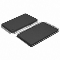
AT91SAM7SE256-AU Atmel, AT91SAM7SE256-AU Datasheet - Page 380

AT91SAM7SE256-AU
Manufacturer Part Number
AT91SAM7SE256-AU
Description
IC ARM7 MCU FLASH 256K 128-LQFP
Manufacturer
Atmel
Series
AT91SAMr
Datasheets
1.AT88SC-SDK1.pdf
(90 pages)
2.AT91SAM7SE256-AU.pdf
(673 pages)
3.AT91SAM7SE32-AU.pdf
(655 pages)
Specifications of AT91SAM7SE256-AU
Core Processor
ARM7
Core Size
16/32-Bit
Speed
55MHz
Connectivity
EBI/EMI, I²C, SPI, SSC, UART/USART, USB
Peripherals
Brown-out Detect/Reset, POR, PWM, WDT
Number Of I /o
88
Program Memory Size
256KB (256K x 8)
Program Memory Type
FLASH
Ram Size
32K x 8
Voltage - Supply (vcc/vdd)
1.65 V ~ 1.95 V
Data Converters
A/D 8x10b
Oscillator Type
Internal
Operating Temperature
-40°C ~ 85°C
Package / Case
128-LQFP
Processor Series
AT91SAMx
Core
ARM7TDMI
Data Bus Width
32 bit
Data Ram Size
32 KB
Interface Type
SPI, TWI, USART
Maximum Clock Frequency
55 MHz
Number Of Programmable I/os
88
Number Of Timers
2
Operating Supply Voltage
3 V to 3.6 V
Maximum Operating Temperature
+ 85 C
Mounting Style
SMD/SMT
3rd Party Development Tools
JTRACE-ARM-2M, KSK-AT91SAM7S-PL, MDK-ARM, RL-ARM, ULINK2
Development Tools By Supplier
AT91SAM-ICE, AT91-ISP, AT91SAM7SE-EK
Minimum Operating Temperature
- 40 C
On-chip Adc
10 bit, 8 Channel
Controller Family/series
AT91SAM7xxxxx
No. Of I/o's
88
Ram Memory Size
32KB
Cpu Speed
48MHz
No. Of Timers
3
Rohs Compliant
Yes
For Use With
AT91SAM7SE-EK - EVAL BOARD FOR AT91SAM7SEAT91SAM-ICE - EMULATOR FOR AT91 ARM7/ARM9
Lead Free Status / RoHS Status
Lead free / RoHS Compliant
Eeprom Size
-
Lead Free Status / Rohs Status
Lead free / RoHS Compliant
Available stocks
Company
Part Number
Manufacturer
Quantity
Price
Company:
Part Number:
AT91SAM7SE256-AU
Manufacturer:
ATMEL
Quantity:
165
- Current page: 380 of 655
- Download datasheet (8Mb)
33.7
33.7.1
33.7.2
33.7.3
33.7.4
380
Master Mode
AT91SAM7SE512/256/32 Preliminary
Definition
Application Block Diagram
Programming Master Mode
Transmitting Data
The Master is the device which starts a transfer, generates a clock and stops it.
Figure 33-5. Master Mode Typical Application Block Diagram
The following registers have to be programmed before entering Master mode:
After the master initiates a Start condition, it sends a 7-bit slave address, configured in the Mas-
ter Mode register (DADR in TWI_MMR), to notify the slave device. The bit following the slave
address indicates the transfer direction (write or read). If this bit is 0, it indicates a write operation
(transmit operation). If the bit is 1, it indicates a request for data read (receive operation).
The TWI transfers require the slave to acknowledge each received byte. During the acknowl-
edge clock pulse, the master releases the data line (HIGH), enabling the slave to pull it down in
order to generate the acknowledge. The master polls the data line during this clock pulse and
sets the NACK bit in the status register if the slave does not acknowledge the byte. As with the
other status bits, an interrupt can be generated if enabled in the interrupt enable register
(TWI_IER). After writing in the transmit-holding register (TWI_THR), the transmission will start
as soon as the bus is free. The data is shifted in the internal shifter and when an acknowledge is
detected, the TXRDY bit is set until a new write in the TWI_THR (see
The master generates a stop condition to end the transfer.
1. DADR (+ IADRSZ + IADR if a 10 bit device is addressed): The device address is used
2. CKDIV + CHDIV + CLDIV: Clock Waveform.
3. SVDIS: Disable the slave mode.
4. MSEN: Enable the master mode.
AT91 (Host)
with TWI
to access slave devices in read or write mode.
Figure 33-7 on page
6222B–ATARM–26-Mar-07
381).
Related parts for AT91SAM7SE256-AU
Image
Part Number
Description
Manufacturer
Datasheet
Request
R

Part Number:
Description:
EVAL BOARD FOR AT91SAM7SE
Manufacturer:
Atmel
Datasheet:

Part Number:
Description:
KIT EVAL FOR ARM AT91SAM7S
Manufacturer:
Atmel
Datasheet:

Part Number:
Description:
MCU, MPU & DSP Development Tools KICKSTART KIT ATMEL AT91SAM7S
Manufacturer:
IAR Systems

Part Number:
Description:
MCU ARM9 64K SRAM 144-LFBGA
Manufacturer:
Atmel
Datasheet:

Part Number:
Description:
IC ARM7 MCU FLASH 256K 100LQFP
Manufacturer:
Atmel
Datasheet:

Part Number:
Description:
IC ARM9 MPU 217-LFBGA
Manufacturer:
Atmel
Datasheet:

Part Number:
Description:
MCU ARM9 ULTRA LOW PWR 217-LFBGA
Manufacturer:
Atmel
Datasheet:

Part Number:
Description:
MCU ARM9 324-TFBGA
Manufacturer:
Atmel
Datasheet:

Part Number:
Description:
IC MCU ARM9 SAMPLING 217CBGA
Manufacturer:
Atmel
Datasheet:

Part Number:
Description:
IC ARM9 MCU 217-LFBGA
Manufacturer:
Atmel
Datasheet:

Part Number:
Description:
IC ARM9 MCU 208-PQFP
Manufacturer:
Atmel
Datasheet:

Part Number:
Description:
MCU ARM 512K HS FLASH 100-LQFP
Manufacturer:
Atmel
Datasheet:

Part Number:
Description:
MCU ARM 512K HS FLASH 100-TFBGA
Manufacturer:
Atmel
Datasheet:

Part Number:
Description:
IC ARM9 MCU 200 MHZ 324-TFBGA
Manufacturer:
Atmel
Datasheet:

Part Number:
Description:
IC ARM MCU 16BIT 128K 256BGA
Manufacturer:
Atmel
Datasheet:


