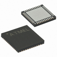
ATMEGA162L-8MI Atmel, ATMEGA162L-8MI Datasheet - Page 15

ATMEGA162L-8MI
Manufacturer Part Number
ATMEGA162L-8MI
Description
IC MCU AVR 16K 3V 8MHZ 44-QFN
Manufacturer
Atmel
Series
AVR® ATmegar
Specifications of ATMEGA162L-8MI
Core Processor
AVR
Core Size
8-Bit
Speed
8MHz
Connectivity
EBI/EMI, SPI, UART/USART
Peripherals
Brown-out Detect/Reset, POR, PWM, WDT
Number Of I /o
35
Program Memory Size
16KB (8K x 16)
Program Memory Type
FLASH
Eeprom Size
512 x 8
Ram Size
1K x 8
Voltage - Supply (vcc/vdd)
2.7 V ~ 5.5 V
Oscillator Type
Internal
Operating Temperature
-40°C ~ 85°C
Package / Case
44-VQFN Exposed Pad
Lead Free Status / RoHS Status
Contains lead / RoHS non-compliant
Data Converters
-
- Current page: 15 of 289
- Download datasheet (3Mb)
AVR ATmega162
Memories
In-System
Reprogrammable Flash
Program Memory
2513C–AVR–09/02
This section describes the different memories in the ATmega162. The AVR architecture
has two main memory spaces, the Data Memory and the Program Memory space. In
addition, the ATmega162 features an EEPROM Memory for data storage. All three
memory spaces are linear and regular.
The ATmega162 contains 16K bytes On-chip In-System Reprogrammable Flash mem-
ory for program storage. Since all AVR instructions are 16 or 32 bits wide, the Flash is
organized as 8K x 16. For software security, the Flash Program memory space is
divided into two sections, Boot Program section and Application Program section.
The Flash memory has an endurance of at least 10,000 write/erase cycles. The
ATmega162 Program Counter (PC) is 13 bits wide, thus addressing the 8K program
memory locations. The operation of Boot Program section and associated Boot Lock
bits for software protection are described in detail in “Boot Loader Support – Read-
While-Write Self-programming” on page 214. “Memory Programming” on page 228 con-
tains a detailed description on Flash data serial downloading using the SPI pins or the
JTAG interface.
Constant tables can be allocated within the entire program memory address space (see
the LPM – Load Program Memory instruction description).
Timing diagrams for instruction fetch and execution are presented in “Instruction Execu-
tion Timing” on page 12.
Figure 8. Program Memory Map
Note:
1. The address reflects word addresses.
Application Flash Section
Boot Flash Section
Program Memory
(1)
ATmega162(V/U/L)
0x0000
0x1FFF
15
Related parts for ATMEGA162L-8MI
Image
Part Number
Description
Manufacturer
Datasheet
Request
R

Part Number:
Description:
Manufacturer:
Atmel Corporation
Datasheet:

Part Number:
Description:
IC AVR MCU 16K 16MHZ 5V 44TQFP
Manufacturer:
Atmel
Datasheet:

Part Number:
Description:
IC AVR MCU 16K 16MHZ 5V 40DIP
Manufacturer:
Atmel
Datasheet:

Part Number:
Description:
IC AVR MCU 16K 16MHZ 5V 44-QFN
Manufacturer:
Atmel
Datasheet:

Part Number:
Description:
IC MCU AVR 16K 5V 16MHZ 44-TQFP
Manufacturer:
Atmel
Datasheet:

Part Number:
Description:
IC MCU AVR 16K 5V 16MHZ 44-QFN
Manufacturer:
Atmel
Datasheet:

Part Number:
Description:
MCU AVR 16KB FLASH 16MHZ 44QFN
Manufacturer:
Atmel
Datasheet:

Part Number:
Description:
MCU AVR 16KB FLASH 16MHZ 44TQFP
Manufacturer:
Atmel
Datasheet:

Part Number:
Description:
IC MCU AVR 16K 5V 16MHZ 44-TQFP
Manufacturer:
Atmel
Datasheet:

Part Number:
Description:
IC MCU AVR 16K 5V 16MHZ 44-QFN
Manufacturer:
Atmel
Datasheet:

Part Number:
Description:
IC MCU AVR 16K 5V 16MHZ 40-DIP
Manufacturer:
Atmel
Datasheet:

Part Number:
Description:
IC MCU AVR 16K 5V 16MHZ 40-DIP
Manufacturer:
Atmel
Datasheet:

Part Number:
Description:
IC MCU AVR 16K 5V 16MHZ 44-TQFP
Manufacturer:
Atmel
Datasheet:


