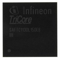
SAF-TC1130-L150EB-G BB Infineon Technologies, SAF-TC1130-L150EB-G BB Datasheet - Page 20

SAF-TC1130-L150EB-G BB
Manufacturer Part Number
SAF-TC1130-L150EB-G BB
Description
IC MCU 32BIT TRICOR 16KB LBGA208
Manufacturer
Infineon Technologies
Series
TC11xxr
Datasheet
1.SAF-TC1130-L100EB-G_BB.pdf
(114 pages)
Specifications of SAF-TC1130-L150EB-G BB
Core Processor
TriCore
Core Size
32-Bit
Speed
150MHz
Connectivity
CAN, EBI/EMI, FIFO, I²C, IrDA, SPI, UART/USART, USB
Peripherals
DMA, POR, PWM, WDT
Number Of I /o
72
Program Memory Type
ROMless
Ram Size
144K x 8
Voltage - Supply (vcc/vdd)
1.43 V ~ 1.58 V
Oscillator Type
External
Operating Temperature
-40°C ~ 85°C
Package / Case
208-LSBGA
Data Bus Width
32 bit
Program Memory Size
32 KB
Data Ram Size
144 KB
Interface Type
3xASC, 2xSSC, I2C, 2xMLI, Ethernet 10, 100 Mbits, s, USB
Maximum Clock Frequency
150 MHz
Number Of Programmable I/os
72
Number Of Timers
9
Operating Supply Voltage
1.5 V, 3.3 V
Maximum Operating Temperature
+ 85 C
Mounting Style
SMD/SMT
Minimum Operating Temperature
- 40 C
Packages
PG-LBGA-208
Max Clock Frequency
150.0 MHz
Sram (incl. Cache)
144.0 KByte
Can Nodes
4
Program Memory
0.0 KByte
Lead Free Status / RoHS Status
Lead free / RoHS Compliant
Eeprom Size
-
Program Memory Size
-
Data Converters
-
Lead Free Status / Rohs Status
Details
Other names
FT1130L150EBGBBXP
SAF-TC1130-L150EB-GBB
SAF-TC1130-L150EB-GBBINTR
SAF-TC1130-L150EB-GBBTR
SAF-TC1130-L150EB-GBBTR
SAFTC1130L150EBBBXT
SP000106119
SP000106538
SP000743584
SAF-TC1130-L150EB-GBB
SAF-TC1130-L150EB-GBBINTR
SAF-TC1130-L150EB-GBBTR
SAF-TC1130-L150EB-GBBTR
SAFTC1130L150EBBBXT
SP000106119
SP000106538
SP000743584
Table 2-1
Symbol
P4
P4.0
P4.1
P4.2
P4.3
P4.4
P4.5
P4.6
P4.7
HDRST
PORST
NMI
Data Sheet
Pin
R8
R9
N7
N6
P6
R7
R6
P5
N5
R5
T7
Pin Definitions and Functions (cont’d)
In
Out
I/O
I
O
I
I
I
O
I
O
O
I
O
O
O
I
I
O
I/O
I
I
PU/
PD
PUC
PUC
PUC
PUC
PUC
PUC
PUC
PUC
PUA
PUC Power-on Reset Input
PUC Non-Maskable Interrupt Input
1)
Functions
Port 4
Port 4 is an 8-bit bi-directional general purpose I/O
port which can be alternatively used for USB, MLI0 and
SCU.
USBCLK
TCLK0B
RCVI
TREADY0B
VPI
TVALID0B
VMI
TDATA0B
VPO
RCLK0B
VMO
RREADY0B
USBOE
RVALID0B
RDATA0B
BRKOUT_A
Hardware Reset Input/Reset Indication Output
Assertion of this bi-directional open-drain pin causes a
synchronous reset of the chip through external
circuitry. This pin must be driven for a minimum 4
clock cycles.
The internal reset circuitry drives this pin in response
to a power-on, hardware, watchdog and power-down
wake-up reset for a specific period of time. For a
software reset, activation of this pin is programmable.
A low level on PORST causes an asynchronous reset
of the entire chip. PORST is a fully asynchronous level
sensitive signal.
A high-to-low transition on this pin causes an
NMI-Trap request to the CPU.
14
differential signal
USB D- CMOS level mirror of
48 MHz input clock
USB data input
USB D+ CMOS level mirror of
differential signal
USB D+ CMOS level output
USB D- CMOS level output
Direction select for transmit or receive
MLI0 receive channel data input B
MLI0 transmit channel clock output B
MLI0 transmit channel ready input B
MLI0 transmit channel valid output B
MLI0 transmit channel data output B
MLI0 receive channel clock input B
MLI0 receive channel ready output B
MLI0 receive channel valid input B
OCDS Break Out A
General Device Information
V1.1, 2008-12
TC1130
f
CPU


