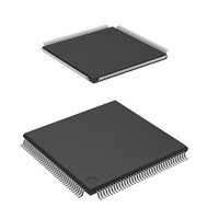
DF2166VT33 Renesas Electronics America, DF2166VT33 Datasheet - Page 6

DF2166VT33
Manufacturer Part Number
DF2166VT33
Description
MCU FLASH 3V 512K 33MHZ 144TQFP
Manufacturer
Renesas Electronics America
Series
H8® H8S/2100r
Datasheet
1.HS2168EPI61H-U.pdf
(876 pages)
Specifications of DF2166VT33
Core Processor
H8S/2000
Core Size
16-Bit
Speed
33MHz
Connectivity
I²C, IrDA, LPC, SCI, SmartCard
Peripherals
POR, PWM, WDT
Number Of I /o
106
Program Memory Size
512KB (512K x 8)
Program Memory Type
FLASH
Ram Size
40K x 8
Voltage - Supply (vcc/vdd)
3 V ~ 3.6 V
Data Converters
A/D 8x10b; D/A 2x8b
Oscillator Type
External
Operating Temperature
-20°C ~ 75°C
Package / Case
144-TQFP, 144-VQFP
Lead Free Status / RoHS Status
Contains lead / RoHS non-compliant
Eeprom Size
-
Available stocks
Company
Part Number
Manufacturer
Quantity
Price
Company:
Part Number:
DF2166VT33V
Manufacturer:
Exar
Quantity:
60
Company:
Part Number:
DF2166VT33V
Manufacturer:
Renesas Electronics America
Quantity:
10 000
Company:
Part Number:
DF2166VT33WV
Manufacturer:
Renesas Electronics America
Quantity:
135
Company:
Part Number:
DF2166VT33WV
Manufacturer:
Renesas Electronics America
Quantity:
10 000
- Current page: 6 of 876
- Download datasheet (5Mb)
General Precautions on Handling of Product
1. Treatment of NC Pins
Note: Do not connect anything to the NC pins.
2. Treatment of Unused Input Pins
Note: Fix all unused input pins to high or low level.
3. Processing before Initialization
Note: When power is first supplied, the product’s state is undefined.
4. Prohibition of Access to Undefined or Reserved Addresses
Note: Access to undefined or reserved addresses is prohibited.
Rev. 3.00, 03/04, page iv of xl
The NC (not connected) pins are either not connected to any of the internal circuitry or are
used as test pins or to reduce noise. If something is connected to the NC pins, the
operation of the LSI is not guaranteed.
Generally, the input pins of CMOS products are high-impedance input pins. If unused pins
are in their open states, intermediate levels are induced by noise in the vicinity, a pass-
through current flows internally, and a malfunction may occur.
The states of internal circuits are undefined until full power is supplied throughout the
chip and a low level is input on the reset pin. During the period where the states are
undefined, the register settings and the output state of each pin are also undefined. Design
your system so that it does not malfunction because of processing while it is in this
undefined state. For those products which have a reset function, reset the LSI immediately
after the power supply has been turned on.
The undefined or reserved addresses may be used to expand functions, or test registers
may have been be allocated to these addresses. Do not access these registers; the system’s
operation is not guaranteed if they are accessed.
Related parts for DF2166VT33
Image
Part Number
Description
Manufacturer
Datasheet
Request
R

Part Number:
Description:
0.6mm Pitch Board-to-Fine-Coaxial Cable Connectors
Manufacturer:
Hirose Electric
Datasheet:

Part Number:
Description:
0.6mm Pitch Board-to-fine-coaxial Cable Connectors
Manufacturer:
Hirose Electric
Datasheet:

Part Number:
Description:
0.6mm Pitch Board-to-fine-coaxial Cable Connectors
Manufacturer:
Hirose Electric
Datasheet:

Part Number:
Description:
Right angle, Two-piece for fine coaxial cable, Discrete wire connectors; HRS No: 687-0001-5 56; No. of Positions: 20; Connector Type: Board mounting; Contact Gender: Female; Contact Spacing (mm): 0.6; Terminal Pitch (mm): 0.6; PCB Mount Type: SMT; Cu
Manufacturer:
Hirose Electric

Part Number:
Description:
0.6mm Pitch Board-to-fine-coaxial Cable Connectors
Manufacturer:
Hirose Electric
Datasheet:

Part Number:
Description:
0.6mm Pitch Board-to-Fine-Coaxial Cable Connectors
Manufacturer:
HIROSE [Hirose Electric]
Datasheet:

Part Number:
Description:
KIT STARTER FOR M16C/29
Manufacturer:
Renesas Electronics America
Datasheet:

Part Number:
Description:
KIT STARTER FOR R8C/2D
Manufacturer:
Renesas Electronics America
Datasheet:

Part Number:
Description:
R0K33062P STARTER KIT
Manufacturer:
Renesas Electronics America
Datasheet:

Part Number:
Description:
KIT STARTER FOR R8C/23 E8A
Manufacturer:
Renesas Electronics America
Datasheet:

Part Number:
Description:
KIT STARTER FOR R8C/25
Manufacturer:
Renesas Electronics America
Datasheet:

Part Number:
Description:
KIT STARTER H8S2456 SHARPE DSPLY
Manufacturer:
Renesas Electronics America
Datasheet:

Part Number:
Description:
KIT STARTER FOR R8C38C
Manufacturer:
Renesas Electronics America
Datasheet:

Part Number:
Description:
KIT STARTER FOR R8C35C
Manufacturer:
Renesas Electronics America
Datasheet:

Part Number:
Description:
KIT STARTER FOR R8CL3AC+LCD APPS
Manufacturer:
Renesas Electronics America
Datasheet:


