HD6473228F10V Renesas Electronics America, HD6473228F10V Datasheet - Page 88
HD6473228F10V
Manufacturer Part Number
HD6473228F10V
Description
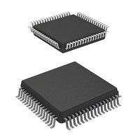
MCU 5V 32K,PB-FREE 64-QFP
Manufacturer
Renesas Electronics America
Series
H8® H8/325r
Datasheet
1.HD6413238F10.pdf
(301 pages)
Specifications of HD6473228F10V
Core Processor
H8/300
Core Size
8-Bit
Speed
10MHz
Connectivity
SCI, UART/USART
Number Of I /o
53
Program Memory Size
8KB (8K x 8)
Program Memory Type
OTP
Ram Size
256 x 8
Voltage - Supply (vcc/vdd)
4.5 V ~ 5.5 V
Oscillator Type
External
Operating Temperature
-20°C ~ 75°C
Package / Case
64-QFP
Lead Free Status / RoHS Status
Lead free / RoHS Compliant
Eeprom Size
-
Data Converters
-
Peripherals
-
Available stocks
Company
Part Number
Manufacturer
Quantity
Price
Company:

Part Number:
HD6473228F10V
Manufacturer:
Renesas Electronics America
Quantity:
10 000


Table 5-3 details the port 1 registers.
Table 5-3. Port 1 Registers
Name
Port 1 data direction register
Port 1 data register
Port 1 Data Direction Register (P1DDR)—H’FFB0
Bit
Mode 1
Modes 2 and 3
P1DDR is an 8-bit register that selects the direction of each pin in port 1. A pin functions as an
output pin if the corresponding bit in P1DDR is set to 1, and as an input pin if the bit is cleared to 0.
Port 1 Data Register (P1DR)—H’FFB2
Bit
Initial value
Read/Write
P1DR is an 8-bit register containing output data for pins P1
ups.
MOS Pull-Ups: Are available for input pins in modes 2 and 3. Software can turn on the MOS pull-
up by writing a 1 in P1DR, and turn it off by writing a 0. The pull-ups are automatically turned off
for output pins in modes 2 and 3, and for all pins in mode 1.
Mode 1: In mode 1 (expanded mode without on-chip ROM), port 1 is automatically used for
address output. The port 1 data direction register is unwritable. All bits in P1DDR are automatically
set to 1 and cannot be cleared to 0.
Initial value
Read/Write
Initial value
Read/Write
P1
R/W
7
P1
—
W
DDR P1
7
1
0
7
0
7
R/W
6
P1
—
W
DDR P1
6
1
0
6
0
Abbreviation
P1DDR
P1DR
6
R/W
5
P1
—
W
DDR P1
5
1
0
5
0
5
R/W
79
Read/Write
W
R/W
4
P1
—
W
DDR P1
4
1
0
4
0
4
R/W
3
P1
7
—
W
DDR P1
3
1
0
3
0
to P1
3
Initial value
H’FF (mode 1)
H’00 (modes 2 and 3)
H’00
0
, and controlling their input pull-
R/W
2
P1
—
W
DDR P1
2
1
0
2
0
2
R/W
1
P1
—
W
DDR P1
1
1
0
1
0
1
R/W
0
P1
—
W
DDR
0
1
0
0
0
Address
H’FFB0
H’FFB2
0
Related parts for HD6473228F10V
Image
Part Number
Description
Manufacturer
Datasheet
Request
R

Part Number:
Description:
KIT STARTER FOR M16C/29
Manufacturer:
Renesas Electronics America
Datasheet:

Part Number:
Description:
KIT STARTER FOR R8C/2D
Manufacturer:
Renesas Electronics America
Datasheet:

Part Number:
Description:
R0K33062P STARTER KIT
Manufacturer:
Renesas Electronics America
Datasheet:

Part Number:
Description:
KIT STARTER FOR R8C/23 E8A
Manufacturer:
Renesas Electronics America
Datasheet:

Part Number:
Description:
KIT STARTER FOR R8C/25
Manufacturer:
Renesas Electronics America
Datasheet:

Part Number:
Description:
KIT STARTER H8S2456 SHARPE DSPLY
Manufacturer:
Renesas Electronics America
Datasheet:

Part Number:
Description:
KIT STARTER FOR R8C38C
Manufacturer:
Renesas Electronics America
Datasheet:

Part Number:
Description:
KIT STARTER FOR R8C35C
Manufacturer:
Renesas Electronics America
Datasheet:

Part Number:
Description:
KIT STARTER FOR R8CL3AC+LCD APPS
Manufacturer:
Renesas Electronics America
Datasheet:
Part Number:
Description:
KIT STARTER FOR RX610
Manufacturer:
Renesas Electronics America
Datasheet:

Part Number:
Description:
KIT STARTER FOR R32C/118
Manufacturer:
Renesas Electronics America
Datasheet:

Part Number:
Description:
KIT DEV RSK-R8C/26-29
Manufacturer:
Renesas Electronics America
Datasheet:

Part Number:
Description:
KIT STARTER FOR SH7124
Manufacturer:
Renesas Electronics America
Datasheet:

Part Number:
Description:
KIT STARTER FOR H8SX/1622
Manufacturer:
Renesas Electronics America
Datasheet:

Part Number:
Description:
KIT DEV FOR SH7203
Manufacturer:
Renesas Electronics America
Datasheet: