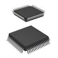
HD6473228F10V Renesas Electronics America, HD6473228F10V Datasheet - Page 110

HD6473228F10V
Manufacturer Part Number
HD6473228F10V
Description
MCU 5V 32K,PB-FREE 64-QFP
Manufacturer
Renesas Electronics America
Series
H8® H8/325r
Datasheet
1.HD6413238F10.pdf
(301 pages)
Specifications of HD6473228F10V
Core Processor
H8/300
Core Size
8-Bit
Speed
10MHz
Connectivity
SCI, UART/USART
Number Of I /o
53
Program Memory Size
8KB (8K x 8)
Program Memory Type
OTP
Ram Size
256 x 8
Voltage - Supply (vcc/vdd)
4.5 V ~ 5.5 V
Oscillator Type
External
Operating Temperature
-20°C ~ 75°C
Package / Case
64-QFP
Lead Free Status / RoHS Status
Lead free / RoHS Compliant
Eeprom Size
-
Data Converters
-
Peripherals
-
Available stocks
Company
Part Number
Manufacturer
Quantity
Price
Company:
Part Number:
HD6473228F10V
Manufacturer:
Renesas Electronics America
Quantity:
10 000
- Current page: 110 of 301
- Download datasheet (2Mb)
MOS Pull-Ups: Are available for input pins, including pins used for input of timer or interrupt
signals. Software can turn the MOS pull-up on by writing a 1 in P6DR, and turn it off by writing a
0. The pull-ups are automatically turned off for output pins.
Pins P6
output, or for input of free-running timer clock and input capture signals. When a pin is used for
free-running timer input, its P6DDR bit should be cleared to 0; otherwise the free-running timer
will receive the value in P6DR. If input pull-up is not desired, the P6DR bit should also be cleared
to 0.
Pin P6
compare signals (FTOA and FTOB) of the free-running timer. When used for FTOA or FTOB
output, these pins are unaffected by the values in P6DDR and P6DR, and their MOS pull-ups are
automatically turned off.
Pins P6
request signals (IRQ
bits should normally be cleared to 0, so that the value in P6DR will not generate interrupts.
Reset and Hardware Standby Mode: P6DDR and P6DR are cleared to all 0. Timer output and
interrupt request input are disabled. All pins are placed in the input port (high-impedance) state
with the MOS pull-ups off.
Software Standby Mode: The free-running timer control registers are initialized but P6DDR,
P6DR, and the interrupt control registers remain in their previous states. All pins become input or
output port pins or interrupt request pins depending on the settings of P6DDR and the IRQ enable
register. Output pins output the values in P6DR. The MOS pull-ups of input pins are on or off
depending on the values in P6DR.
Figures 5-11 to 5-13 shows schematic diagrams of port 6.
1
0
4
and P6
and P6
to P6
6
: These pins can be used for general-purpose input or output, or input of interrupt
2
3
: These pins can be used for general-purpose input or output, or for the output
: As indicated in table 5-12, these pins can be used for general-purpose input or
0
to IRQ
2
). When they are used for interrupt request input, their data direction
101
Related parts for HD6473228F10V
Image
Part Number
Description
Manufacturer
Datasheet
Request
R

Part Number:
Description:
KIT STARTER FOR M16C/29
Manufacturer:
Renesas Electronics America
Datasheet:

Part Number:
Description:
KIT STARTER FOR R8C/2D
Manufacturer:
Renesas Electronics America
Datasheet:

Part Number:
Description:
R0K33062P STARTER KIT
Manufacturer:
Renesas Electronics America
Datasheet:

Part Number:
Description:
KIT STARTER FOR R8C/23 E8A
Manufacturer:
Renesas Electronics America
Datasheet:

Part Number:
Description:
KIT STARTER FOR R8C/25
Manufacturer:
Renesas Electronics America
Datasheet:

Part Number:
Description:
KIT STARTER H8S2456 SHARPE DSPLY
Manufacturer:
Renesas Electronics America
Datasheet:

Part Number:
Description:
KIT STARTER FOR R8C38C
Manufacturer:
Renesas Electronics America
Datasheet:

Part Number:
Description:
KIT STARTER FOR R8C35C
Manufacturer:
Renesas Electronics America
Datasheet:

Part Number:
Description:
KIT STARTER FOR R8CL3AC+LCD APPS
Manufacturer:
Renesas Electronics America
Datasheet:

Part Number:
Description:
KIT STARTER FOR RX610
Manufacturer:
Renesas Electronics America
Datasheet:

Part Number:
Description:
KIT STARTER FOR R32C/118
Manufacturer:
Renesas Electronics America
Datasheet:

Part Number:
Description:
KIT DEV RSK-R8C/26-29
Manufacturer:
Renesas Electronics America
Datasheet:

Part Number:
Description:
KIT STARTER FOR SH7124
Manufacturer:
Renesas Electronics America
Datasheet:

Part Number:
Description:
KIT STARTER FOR H8SX/1622
Manufacturer:
Renesas Electronics America
Datasheet:

Part Number:
Description:
KIT DEV FOR SH7203
Manufacturer:
Renesas Electronics America
Datasheet:


