DF71241D50FPV Renesas Electronics America, DF71241D50FPV Datasheet - Page 612
DF71241D50FPV
Manufacturer Part Number
DF71241D50FPV
Description
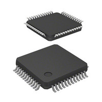
MCU RISC FLASH 5V 32K 48-LQFP
Manufacturer
Renesas Electronics America
Series
SuperH® SH Tinyr
Datasheet
1.DF71243N50FPV.pdf
(794 pages)
Specifications of DF71241D50FPV
Core Processor
SH-2
Core Size
32-Bit
Speed
50MHz
Connectivity
SCI
Peripherals
POR, PWM, WDT
Number Of I /o
23
Program Memory Size
32KB (32K x 8)
Program Memory Type
FLASH
Ram Size
8K x 8
Voltage - Supply (vcc/vdd)
4 V ~ 5.5 V
Data Converters
A/D 8x10b
Oscillator Type
External
Operating Temperature
-40°C ~ 85°C
Package / Case
48-LQFP
Lead Free Status / RoHS Status
Lead free / RoHS Compliant
Eeprom Size
-
Available stocks
Company
Part Number
Manufacturer
Quantity
Price
Company:

Part Number:
DF71241D50FPV
Manufacturer:
Renesas Electronics America
Quantity:
10 000


Rev. 5.00 Mar. 06, 2009 Page 592 of 770
REJ09B0243-0500
Bit
0
Bit Name
SCO
Initial
Value
0
R/W
(R)/W
Description
Source Program Copy Operation
Requests the on-chip programming/erasing program to
be downloaded to the on-chip RAM.
When this bit is set to 1, the on-chip program which is
selected by FPCS/FECS is automatically downloaded in
the on-chip RAM area specified by FTDAR.
In order to set this bit to 1, H'A5 must be written to
FKEY and this operation must be in the on-chip RAM.
Four NOP instructions must be executed immediately
after setting this bit to 1.
For interrupts during download, see section 17.7.1,
Interrupts during Programming/Erasing. For the
download time, see section 17.7.2, Other Notes.
Since this bit is cleared to 0 when download is
completed, this bit cannot be read as 1.
Download by setting the SCO bit to 1 requires a special
interrupt processing that performs bank switching to the
on-chip program storage area. Therefore, before
issuing a download request (SCO = 1), set VBR to
H'84000000. Otherwise, the CPU gets out of control.
Once download end is confirmed, VBR can be changed
to any other value.
The mode in which the FWE pin is high must be used
when using the SCO function.
0: Download of the on-chip programming/erasing
[Clearing condition]
When download is completed
1: Request that the on-chip programming/erasing
[Setting conditions]
When all of the following conditions are satisfied and 1
is written to this bit
•
•
program to the on-chip RAM is not executed.
program is downloaded to the on-chip RAM is
generated
FKEY is written to H'A5
During execution in the on-chip RAM
Related parts for DF71241D50FPV
Image
Part Number
Description
Manufacturer
Datasheet
Request
R

Part Number:
Description:
KIT STARTER FOR M16C/29
Manufacturer:
Renesas Electronics America
Datasheet:

Part Number:
Description:
KIT STARTER FOR R8C/2D
Manufacturer:
Renesas Electronics America
Datasheet:

Part Number:
Description:
R0K33062P STARTER KIT
Manufacturer:
Renesas Electronics America
Datasheet:

Part Number:
Description:
KIT STARTER FOR R8C/23 E8A
Manufacturer:
Renesas Electronics America
Datasheet:

Part Number:
Description:
KIT STARTER FOR R8C/25
Manufacturer:
Renesas Electronics America
Datasheet:

Part Number:
Description:
KIT STARTER H8S2456 SHARPE DSPLY
Manufacturer:
Renesas Electronics America
Datasheet:

Part Number:
Description:
KIT STARTER FOR R8C38C
Manufacturer:
Renesas Electronics America
Datasheet:

Part Number:
Description:
KIT STARTER FOR R8C35C
Manufacturer:
Renesas Electronics America
Datasheet:

Part Number:
Description:
KIT STARTER FOR R8CL3AC+LCD APPS
Manufacturer:
Renesas Electronics America
Datasheet:
Part Number:
Description:
KIT STARTER FOR RX610
Manufacturer:
Renesas Electronics America
Datasheet:

Part Number:
Description:
KIT STARTER FOR R32C/118
Manufacturer:
Renesas Electronics America
Datasheet:

Part Number:
Description:
KIT DEV RSK-R8C/26-29
Manufacturer:
Renesas Electronics America
Datasheet:

Part Number:
Description:
KIT STARTER FOR SH7124
Manufacturer:
Renesas Electronics America
Datasheet:

Part Number:
Description:
KIT STARTER FOR H8SX/1622
Manufacturer:
Renesas Electronics America
Datasheet:

Part Number:
Description:
KIT DEV FOR SH7203
Manufacturer:
Renesas Electronics America
Datasheet: