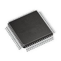
MC908AZ60AVFUER Freescale Semiconductor, MC908AZ60AVFUER Datasheet - Page 356

MC908AZ60AVFUER
Manufacturer Part Number
MC908AZ60AVFUER
Description
IC MCU 64K FLASH 8.4MHZ 64-QFP
Manufacturer
Freescale Semiconductor
Series
HC08r
Datasheet
1.MC908AZ60ACFUER.pdf
(414 pages)
Specifications of MC908AZ60AVFUER
Core Processor
HC08
Core Size
8-Bit
Speed
8.4MHz
Connectivity
CAN, SCI, SPI
Peripherals
LVD, POR, PWM
Number Of I /o
52
Program Memory Size
60KB (60K x 8)
Program Memory Type
FLASH
Eeprom Size
1K x 8
Ram Size
2K x 8
Voltage - Supply (vcc/vdd)
4.5 V ~ 5.5 V
Data Converters
A/D 15x8b
Oscillator Type
Internal
Operating Temperature
-40°C ~ 105°C
Package / Case
64-QFP
Processor Series
HC08AZ
Core
HC08
Data Bus Width
8 bit
Data Ram Size
2 KB
Interface Type
SCI, SPI
Maximum Clock Frequency
8.4 MHz
Number Of Programmable I/os
52
Number Of Timers
8
Maximum Operating Temperature
+ 105 C
Mounting Style
SMD/SMT
Development Tools By Supplier
FSICEBASE, M68CBL05CE, ZK-HC08AX-A, M68EM08AS/AZ60AE
Minimum Operating Temperature
- 40 C
On-chip Adc
8 bit, 15 Channel
Lead Free Status / RoHS Status
Lead free / RoHS Compliant
Available stocks
Company
Part Number
Manufacturer
Quantity
Price
Company:
Part Number:
MC908AZ60AVFUER
Manufacturer:
Freescale Semiconductor
Quantity:
10 000
- Current page: 356 of 414
- Download datasheet (5Mb)
Byte Data Link Controller (BDLC)
IE— Interrupt Enable Bit
WCM — Wait Clock Mode Bit
27.6.3 BDLC Control Register 2
This register controls transmitter operations of the BDLC. It is recommended that BSET and BCLR
instructions be used to manipulate data in this register to ensure that the register’s content does not
change inadvertently.
ALOOP — Analog Loopback Mode Bit
356
This bit determines whether the BDLC will generate CPU interrupt requests in run mode. It does not
affect CPU interrupt requests when exiting the BDLC stop or BDLC wait modes. Interrupt requests will
be maintained until all of the interrupt request sources are cleared by performing the specified actions
upon the BDLC’s registers. Interrupts that were pending at the time that this bit is cleared may be lost.
If the programmer does not wish to use the interrupt capability of the BDLC, the BDLC state vector
register (BSVR) can be polled periodically by the programmer to determine BDLC states. See
BDLC State Vector Register
This bit determines the operation of the BDLC during CPU wait mode. See Stop Mode and Wait Mode
for more details on its use.
This bit determines whether the J1850 bus will be driven by the analog physical interface’s final drive
stage. The programmer can use this bit to reset the BDLC state machine to a known state after the
off-chip analog transceiver is placed in loopback mode. When the user clears ALOOP, to indicate that
1 = Enable interrupt requests from BDLC
0 = Disable interrupt requests from BDLC
1 = Stop BDLC internal clocks during CPU wait mode
0 = Run BDLC internal clocks during CPU wait mode
Address:
Reset:
Read:
Write:
MC68HC908AZ60A • MC68HC908AS60A • MC68HC908AS60E Data Sheet, Rev. 6
f
XCLK
1.049 MHz
2.097 MHz
4.194 MHz
8.389 MHz
1.000 MHz
2.000 MHz
4.000 MHz
8.000 MHz
Frequency
ALOOP
$003D
Bit 7
1
Figure 27-17. BDLC Control Register 2 (BCR2)
DLOOP
for a description of the BSVR.
6
1
Table 27-3. BDLC Rate Selection
R1
0
0
1
1
0
0
1
1
RX4XE
5
0
NBFS
4
0
R0
.
0
1
0
1
0
1
0
1
TEOD
3
0
Division
1
2
4
8
1
2
4
8
TSIFR
2
0
1.049 MHz
1.049 MHz
1.049 MHz
1.049 MHz
1.00 MHz
1.00 MHz
1.00 MHz
1.00 MHz
TMIFR1
f
BDLC
1
0
Freescale Semiconductor
TMIFR0
Bit 0
0
27.6.4
Related parts for MC908AZ60AVFUER
Image
Part Number
Description
Manufacturer
Datasheet
Request
R
Part Number:
Description:
Manufacturer:
Freescale Semiconductor, Inc
Datasheet:
Part Number:
Description:
Manufacturer:
Freescale Semiconductor, Inc
Datasheet:
Part Number:
Description:
Manufacturer:
Freescale Semiconductor, Inc
Datasheet:
Part Number:
Description:
Manufacturer:
Freescale Semiconductor, Inc
Datasheet:
Part Number:
Description:
Manufacturer:
Freescale Semiconductor, Inc
Datasheet:
Part Number:
Description:
Manufacturer:
Freescale Semiconductor, Inc
Datasheet:
Part Number:
Description:
Manufacturer:
Freescale Semiconductor, Inc
Datasheet:
Part Number:
Description:
Manufacturer:
Freescale Semiconductor, Inc
Datasheet:
Part Number:
Description:
Manufacturer:
Freescale Semiconductor, Inc
Datasheet:
Part Number:
Description:
Manufacturer:
Freescale Semiconductor, Inc
Datasheet:
Part Number:
Description:
Manufacturer:
Freescale Semiconductor, Inc
Datasheet:
Part Number:
Description:
Manufacturer:
Freescale Semiconductor, Inc
Datasheet:
Part Number:
Description:
Manufacturer:
Freescale Semiconductor, Inc
Datasheet:
Part Number:
Description:
Manufacturer:
Freescale Semiconductor, Inc
Datasheet:
Part Number:
Description:
Manufacturer:
Freescale Semiconductor, Inc
Datasheet:


