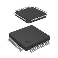
HD64F3672FY Renesas Electronics America, HD64F3672FY Datasheet - Page 19

HD64F3672FY
Manufacturer Part Number
HD64F3672FY
Description
IC H8 MCU FLASH 16K 48QFP
Manufacturer
Renesas Electronics America
Series
H8® H8/300H Tinyr
Datasheet
1.HD64F3672FXV.pdf
(334 pages)
Specifications of HD64F3672FY
Core Processor
H8/300H
Core Size
16-Bit
Speed
16MHz
Connectivity
SCI
Peripherals
PWM, WDT
Number Of I /o
26
Program Memory Size
16KB (16K x 8)
Program Memory Type
FLASH
Ram Size
2K x 8
Voltage - Supply (vcc/vdd)
3 V ~ 5.5 V
Data Converters
A/D 4x10b
Oscillator Type
Internal
Operating Temperature
-20°C ~ 75°C
Package / Case
48-QFP
Lead Free Status / RoHS Status
Contains lead / RoHS non-compliant
Eeprom Size
-
Available stocks
Company
Part Number
Manufacturer
Quantity
Price
Company:
Part Number:
HD64F3672FY
Manufacturer:
Renesas Electronics America
Quantity:
10 000
Company:
Part Number:
HD64F3672FYV
Manufacturer:
Renesas Electronics America
Quantity:
10 000
- Current page: 19 of 334
- Download datasheet (2Mb)
Section 1 Overview
Figure 1.1 Internal Block Diagram ................................................................................................. 2
Figure 1.2 Pin Arrangement (FP-64E)............................................................................................ 3
Figure 1.3 Pin Arrangement (FP-48F, FP-48B).............................................................................. 4
Section 2 CPU
Figure 2.1 Memory Map................................................................................................................. 8
Figure 2.2 CPU Registers ............................................................................................................... 9
Figure 2.3 Usage of General Registers ......................................................................................... 10
Figure 2.4 Relationship between Stack Pointer and Stack Area ................................................... 11
Figure 2.5 General Register Data Formats (1).............................................................................. 13
Figure 2.5 General Register Data Formats (2).............................................................................. 14
Figure 2.6 Memory Data Formats................................................................................................. 15
Figure 2.7 Instruction Formats...................................................................................................... 26
Figure 2.8 Branch Address Specification in Memory Indirect Mode ........................................... 30
Figure 2.9 On-Chip Memory Access Cycle.................................................................................. 32
Figure 2.10 On-Chip Peripheral Module Access Cycle (3-State Access)..................................... 33
Figure 2.11 CPU Operation States................................................................................................ 34
Figure 2.12 State Transitions ........................................................................................................ 35
Figure 2.13 Example of Timer Configuration with Two Registers Allocated to
Section 3 Exception Handling
Figure 3.1 Reset Sequence............................................................................................................ 49
Figure 3.2 Stack Status after Exception Handling ........................................................................ 51
Figure 3.3 Interrupt Sequence....................................................................................................... 52
Figure 3.4 Port Mode Register Setting and Interrupt Request Flag Clearing Procedure .............. 53
Section 4 Address Break
Figure 4.1 Block Diagram of Address Break................................................................................ 55
Figure 4.2 Address Break Interrupt Operation Example (1)......................................................... 59
Figure 4.2 Address Break Interrupt Operation Example (2)......................................................... 60
Figure 4.3 Operation when Condition is not Satisfied in Branch Instruction ............................... 61
Figure 4.4 Operation when Another Interrupt is Accepted at Address Break
Figure 4.5 Operation when the Instruction Set is not Executed and does not
Setting Instruction ....................................................................................................... 62
Branch due to Conditions not Being Satisfied............................................................. 63
Same Address............................................................................................................ 36
Figures
Rev.4.00 Nov. 02, 2005 Page xvii of xxiv
Related parts for HD64F3672FY
Image
Part Number
Description
Manufacturer
Datasheet
Request
R

Part Number:
Description:
(HD64 Series) Hitachi Single-Chip Microcomputer
Manufacturer:
Hitachi Semiconductor
Datasheet:

Part Number:
Description:
KIT STARTER FOR M16C/29
Manufacturer:
Renesas Electronics America
Datasheet:

Part Number:
Description:
KIT STARTER FOR R8C/2D
Manufacturer:
Renesas Electronics America
Datasheet:

Part Number:
Description:
R0K33062P STARTER KIT
Manufacturer:
Renesas Electronics America
Datasheet:

Part Number:
Description:
KIT STARTER FOR R8C/23 E8A
Manufacturer:
Renesas Electronics America
Datasheet:

Part Number:
Description:
KIT STARTER FOR R8C/25
Manufacturer:
Renesas Electronics America
Datasheet:

Part Number:
Description:
KIT STARTER H8S2456 SHARPE DSPLY
Manufacturer:
Renesas Electronics America
Datasheet:

Part Number:
Description:
KIT STARTER FOR R8C38C
Manufacturer:
Renesas Electronics America
Datasheet:

Part Number:
Description:
KIT STARTER FOR R8C35C
Manufacturer:
Renesas Electronics America
Datasheet:

Part Number:
Description:
KIT STARTER FOR R8CL3AC+LCD APPS
Manufacturer:
Renesas Electronics America
Datasheet:

Part Number:
Description:
KIT STARTER FOR RX610
Manufacturer:
Renesas Electronics America
Datasheet:

Part Number:
Description:
KIT STARTER FOR R32C/118
Manufacturer:
Renesas Electronics America
Datasheet:

Part Number:
Description:
KIT DEV RSK-R8C/26-29
Manufacturer:
Renesas Electronics America
Datasheet:

Part Number:
Description:
KIT STARTER FOR SH7124
Manufacturer:
Renesas Electronics America
Datasheet:

Part Number:
Description:
KIT STARTER FOR H8SX/1622
Manufacturer:
Renesas Electronics America
Datasheet:


