HD64F3672FY Renesas Electronics America, HD64F3672FY Datasheet - Page 14
HD64F3672FY
Manufacturer Part Number
HD64F3672FY
Description
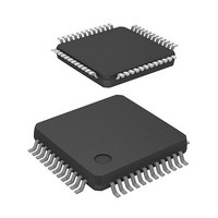
IC H8 MCU FLASH 16K 48QFP
Manufacturer
Renesas Electronics America
Series
H8® H8/300H Tinyr
Datasheet
1.HD64F3672FXV.pdf
(334 pages)
Specifications of HD64F3672FY
Core Processor
H8/300H
Core Size
16-Bit
Speed
16MHz
Connectivity
SCI
Peripherals
PWM, WDT
Number Of I /o
26
Program Memory Size
16KB (16K x 8)
Program Memory Type
FLASH
Ram Size
2K x 8
Voltage - Supply (vcc/vdd)
3 V ~ 5.5 V
Data Converters
A/D 4x10b
Oscillator Type
Internal
Operating Temperature
-20°C ~ 75°C
Package / Case
48-QFP
Lead Free Status / RoHS Status
Contains lead / RoHS non-compliant
Eeprom Size
-
Available stocks
Company
Part Number
Manufacturer
Quantity
Price
Company:

Part Number:
HD64F3672FY
Manufacturer:
Renesas Electronics America
Quantity:
10 000
Company:
Part Number:
HD64F3672FYV
Manufacturer:
Renesas Electronics America
Quantity:
10 000


9.4
9.5
9.6
Section 10 Timer V ........................................................................................... 115
10.1 Features.............................................................................................................................. 115
10.2 Input/Output Pins............................................................................................................... 117
10.3 Register Descriptions......................................................................................................... 117
10.4 Operation ........................................................................................................................... 122
10.5 Timer V Application Examples ......................................................................................... 126
10.6 Usage Notes ....................................................................................................................... 128
Section 11 Timer W........................................................................................... 131
11.1 Features.............................................................................................................................. 131
11.2 Input/Output Pins............................................................................................................... 134
11.3 Register Descriptions......................................................................................................... 134
Rev.4.00 Nov. 02, 2005 Page xii of xxiv
9.3.3
9.3.4
9.3.5
Port 7.................................................................................................................................. 107
9.4.1
9.4.2
9.4.3
Port 8.................................................................................................................................. 110
9.5.1
9.5.2
9.5.3
Port B ................................................................................................................................. 113
9.6.1
10.3.1 Timer Counter V (TCNTV).................................................................................. 117
10.3.2 Time Constant Registers A and B (TCORA, TCORB) ........................................ 118
10.3.3 Timer Control Register V0 (TCRV0) ................................................................... 118
10.3.4 Timer Control/Status Register V (TCSRV) .......................................................... 120
10.3.5 Timer Control Register V1 (TCRV1) ................................................................... 121
10.4.1 Timer V Operation................................................................................................ 122
10.5.1 Pulse Output with Arbitrary Duty Cycle............................................................... 126
10.5.2 Pulse Output with Arbitrary Pulse Width and Delay from TRGV Input .............. 127
11.3.1 Timer Mode Register W (TMRW) ....................................................................... 135
11.3.2 Timer Control Register W (TCRW) ..................................................................... 136
11.3.3 Timer Interrupt Enable Register W (TIERW) ...................................................... 137
11.3.4 Timer Status Register W (TSRW) ........................................................................ 137
11.3.5 Timer I/O Control Register 0 (TIOR0) ................................................................. 139
11.3.6 Timer I/O Control Register 1 (TIOR1) ................................................................. 140
Port Data Register 5 (PDR5) ................................................................................ 104
Port Pull-Up Control Register 5 (PUCR5)............................................................ 105
Pin Functions ........................................................................................................ 105
Port Control Register 7 (PCR7) ............................................................................ 108
Port Data Register 7 (PDR7) ................................................................................ 108
Pin Functions ........................................................................................................ 109
Port Control Register 8 (PCR8) ............................................................................ 110
Port Data Register 8 (PDR8) ................................................................................ 111
Pin Functions ........................................................................................................ 111
Port Data Register B (PDRB) ............................................................................... 114
Related parts for HD64F3672FY
Image
Part Number
Description
Manufacturer
Datasheet
Request
R

Part Number:
Description:
(HD64 Series) Hitachi Single-Chip Microcomputer
Manufacturer:
Hitachi Semiconductor
Datasheet:

Part Number:
Description:
KIT STARTER FOR M16C/29
Manufacturer:
Renesas Electronics America
Datasheet:

Part Number:
Description:
KIT STARTER FOR R8C/2D
Manufacturer:
Renesas Electronics America
Datasheet:

Part Number:
Description:
R0K33062P STARTER KIT
Manufacturer:
Renesas Electronics America
Datasheet:

Part Number:
Description:
KIT STARTER FOR R8C/23 E8A
Manufacturer:
Renesas Electronics America
Datasheet:

Part Number:
Description:
KIT STARTER FOR R8C/25
Manufacturer:
Renesas Electronics America
Datasheet:

Part Number:
Description:
KIT STARTER H8S2456 SHARPE DSPLY
Manufacturer:
Renesas Electronics America
Datasheet:

Part Number:
Description:
KIT STARTER FOR R8C38C
Manufacturer:
Renesas Electronics America
Datasheet:

Part Number:
Description:
KIT STARTER FOR R8C35C
Manufacturer:
Renesas Electronics America
Datasheet:

Part Number:
Description:
KIT STARTER FOR R8CL3AC+LCD APPS
Manufacturer:
Renesas Electronics America
Datasheet:
Part Number:
Description:
KIT STARTER FOR RX610
Manufacturer:
Renesas Electronics America
Datasheet:

Part Number:
Description:
KIT STARTER FOR R32C/118
Manufacturer:
Renesas Electronics America
Datasheet:

Part Number:
Description:
KIT DEV RSK-R8C/26-29
Manufacturer:
Renesas Electronics America
Datasheet:

Part Number:
Description:
KIT STARTER FOR SH7124
Manufacturer:
Renesas Electronics America
Datasheet:

Part Number:
Description:
KIT STARTER FOR H8SX/1622
Manufacturer:
Renesas Electronics America
Datasheet: