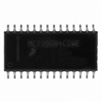
MC908GR4CDWE Freescale Semiconductor, MC908GR4CDWE Datasheet - Page 83

MC908GR4CDWE
Manufacturer Part Number
MC908GR4CDWE
Description
IC MCU 4K FLASH 8MHZ 28-SOIC
Manufacturer
Freescale Semiconductor
Series
HC08r
Specifications of MC908GR4CDWE
Core Processor
HC08
Core Size
8-Bit
Speed
8MHz
Connectivity
SCI, SPI
Peripherals
LVD, POR, PWM
Number Of I /o
17
Program Memory Size
4KB (4K x 8)
Program Memory Type
FLASH
Ram Size
384 x 8
Voltage - Supply (vcc/vdd)
2.7 V ~ 5.5 V
Data Converters
A/D 6x8b
Oscillator Type
Internal
Operating Temperature
-40°C ~ 85°C
Package / Case
28-SOIC (7.5mm Width)
Controller Family/series
HC08
No. Of I/o's
21
Ram Memory Size
384Byte
Cpu Speed
8MHz
No. Of Timers
1
Embedded Interface Type
I2C, SCI, SPI
Rohs Compliant
Yes
Processor Series
HC08GR
Core
HC08
Data Bus Width
8 bit
Data Ram Size
384 B
Interface Type
SCI, SPI
Maximum Clock Frequency
8.2 MHz
Number Of Programmable I/os
21
Number Of Timers
3
Maximum Operating Temperature
+ 85 C
Mounting Style
SMD/SMT
Development Tools By Supplier
FSICEBASE, DEMO908GZ60E, M68CBL05CE, M68EML08GPGTE
Minimum Operating Temperature
- 40 C
On-chip Adc
8 bit, 6 Channel
Lead Free Status / RoHS Status
Lead free / RoHS Compliant
Eeprom Size
-
Lead Free Status / Rohs Status
Details
- Current page: 83 of 408
- Download datasheet (4Mb)
5.4.5 Accuracy and Precision
5.5 Interrupts
5.6 Low-Power Modes
5.6.1 Wait Mode
5.6.2 Stop Mode
5.7 I/O Signals
MC68HC908GR8 — Rev 4.0
MOTOROLA
The conversion process is monotonic and has no missing codes.
When the AIEN bit is set, the ADC module is capable of generating CPU
interrupts after each ADC conversion. A CPU interrupt is generated if the
COCO/IDMAS bit is at logic 0. If COCO/IDMAS bit is set, a DMA interrupt
is generated. The COCO/IDMAS bit is not used as a conversion
complete flag when interrupts are enabled.
The WAIT and STOP instruction can put the MCU in low power-
consumption standby modes.
The ADC continues normal operation during wait mode. Any enabled
CPU interrupt request from the ADC can bring the MCU out of wait
mode. If the ADC is not required to bring the MCU out of wait mode,
power down the ADC by setting ADCH4–ADCH0 bits in the ADC status
and control register before executing the WAIT instruction.
The ADC module is inactive after the execution of a STOP instruction.
Any pending conversion is aborted. ADC conversions resume when the
MCU exits stop mode after an external interrupt. Allow one conversion
cycle to stabilize the analog circuitry.
The ADC module has six pins shared with port B,
PTB5/AD5–PTB0/ATD0.
Freescale Semiconductor, Inc.
For More Information On This Product,
Analog-to-Digital Converter (ADC)
Go to: www.freescale.com
Analog-to-Digital Converter (ADC)
Technical Data
Interrupts
83
Related parts for MC908GR4CDWE
Image
Part Number
Description
Manufacturer
Datasheet
Request
R
Part Number:
Description:
Manufacturer:
Freescale Semiconductor, Inc
Datasheet:
Part Number:
Description:
Manufacturer:
Freescale Semiconductor, Inc
Datasheet:
Part Number:
Description:
Manufacturer:
Freescale Semiconductor, Inc
Datasheet:
Part Number:
Description:
Manufacturer:
Freescale Semiconductor, Inc
Datasheet:
Part Number:
Description:
Manufacturer:
Freescale Semiconductor, Inc
Datasheet:
Part Number:
Description:
Manufacturer:
Freescale Semiconductor, Inc
Datasheet:
Part Number:
Description:
Manufacturer:
Freescale Semiconductor, Inc
Datasheet:
Part Number:
Description:
Manufacturer:
Freescale Semiconductor, Inc
Datasheet:
Part Number:
Description:
Manufacturer:
Freescale Semiconductor, Inc
Datasheet:
Part Number:
Description:
Manufacturer:
Freescale Semiconductor, Inc
Datasheet:
Part Number:
Description:
Manufacturer:
Freescale Semiconductor, Inc
Datasheet:
Part Number:
Description:
Manufacturer:
Freescale Semiconductor, Inc
Datasheet:
Part Number:
Description:
Manufacturer:
Freescale Semiconductor, Inc
Datasheet:
Part Number:
Description:
Manufacturer:
Freescale Semiconductor, Inc
Datasheet:
Part Number:
Description:
Manufacturer:
Freescale Semiconductor, Inc
Datasheet:


