MC908GR4CDWE Freescale Semiconductor, MC908GR4CDWE Datasheet - Page 323
MC908GR4CDWE
Manufacturer Part Number
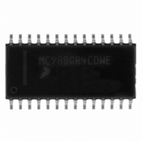
MC908GR4CDWE
Description
IC MCU 4K FLASH 8MHZ 28-SOIC
Manufacturer
Freescale Semiconductor
Series
HC08r
Specifications of MC908GR4CDWE
Core Processor
HC08
Core Size
8-Bit
Speed
8MHz
Connectivity
SCI, SPI
Peripherals
LVD, POR, PWM
Number Of I /o
17
Program Memory Size
4KB (4K x 8)
Program Memory Type
FLASH
Ram Size
384 x 8
Voltage - Supply (vcc/vdd)
2.7 V ~ 5.5 V
Data Converters
A/D 6x8b
Oscillator Type
Internal
Operating Temperature
-40°C ~ 85°C
Package / Case
28-SOIC (7.5mm Width)
Controller Family/series
HC08
No. Of I/o's
21
Ram Memory Size
384Byte
Cpu Speed
8MHz
No. Of Timers
1
Embedded Interface Type
I2C, SCI, SPI
Rohs Compliant
Yes
Processor Series
HC08GR
Core
HC08
Data Bus Width
8 bit
Data Ram Size
384 B
Interface Type
SCI, SPI
Maximum Clock Frequency
8.2 MHz
Number Of Programmable I/os
21
Number Of Timers
3
Maximum Operating Temperature
+ 85 C
Mounting Style
SMD/SMT
Development Tools By Supplier
FSICEBASE, DEMO908GZ60E, M68CBL05CE, M68EML08GPGTE
Minimum Operating Temperature
- 40 C
On-chip Adc
8 bit, 6 Channel
Lead Free Status / RoHS Status
Lead free / RoHS Compliant
Eeprom Size
-
Lead Free Status / Rohs Status
Details


MC68HC908GR8 — Rev 4.0
MOTOROLA
SPRIE — SPI Receiver Interrupt Enable Bit
DMAS —DMA Select Bit
SPMSTR — SPI Master Bit
CPOL — Clock Polarity Bit
CPHA — Clock Phase Bit
SPWOM — SPI Wired-OR Mode Bit
Freescale Semiconductor, Inc.
This read/write bit enables CPU interrupt requests generated by the
SPRF bit. The SPRF bit is set when a byte transfers from the shift
register to the receive data register. Reset clears the SPRIE bit.
This read only bit has no effect on this version of the SPI. This bit
always reads as a 0.
This read/write bit selects master mode operation or slave mode
operation. Reset sets the SPMSTR bit.
This read/write bit determines the logic state of the SPSCK pin
between transmissions. (See
transmit data between SPI modules, the SPI modules must have
identical CPOL values. Reset clears the CPOL bit.
This read/write bit controls the timing relationship between the serial
clock and SPI data. (See
data between SPI modules, the SPI modules must have identical
CPHA values. When CPHA = 0, the SS pin of the slave SPI module
must be set to logic 1 between bytes. See
the CPHA bit.
This read/write bit disables the pullup devices on pins SPSCK, MOSI,
and MISO so that those pins become open-drain outputs.
For More Information On This Product,
1 = SPRF CPU interrupt requests enabled
0 = SPRF CPU interrupt requests disabled
0 = SPRF DMA and SPTE DMA service requests disabled
1 = Master mode
0 = Slave mode
1 = Wired-OR SPSCK, MOSI, and MISO pins
0 = Normal push-pull SPSCK, MOSI, and MISO pins
(SPRF CPU and SPTE CPU interrupt requests enabled)
Serial Peripheral Interface (SPI)
Go to: www.freescale.com
Figure 20-4
Figure 20-4
and
and
Serial Peripheral Interface (SPI)
Figure
Figure
Figure
20-6.) To transmit
20-12. Reset sets
20-6.) To
Technical Data
I/O Registers
323
Related parts for MC908GR4CDWE
Image
Part Number
Description
Manufacturer
Datasheet
Request
R

Part Number:
Description:
Manufacturer:
Freescale Semiconductor, Inc
Datasheet:
Part Number:
Description:
Manufacturer:
Freescale Semiconductor, Inc
Datasheet:
Part Number:
Description:
Manufacturer:
Freescale Semiconductor, Inc
Datasheet:
Part Number:
Description:
Manufacturer:
Freescale Semiconductor, Inc
Datasheet:
Part Number:
Description:
Manufacturer:
Freescale Semiconductor, Inc
Datasheet:
Part Number:
Description:
Manufacturer:
Freescale Semiconductor, Inc
Datasheet:
Part Number:
Description:
Manufacturer:
Freescale Semiconductor, Inc
Datasheet:
Part Number:
Description:
Manufacturer:
Freescale Semiconductor, Inc
Datasheet:
Part Number:
Description:
Manufacturer:
Freescale Semiconductor, Inc
Datasheet:
Part Number:
Description:
Manufacturer:
Freescale Semiconductor, Inc
Datasheet:
Part Number:
Description:
Manufacturer:
Freescale Semiconductor, Inc
Datasheet:
Part Number:
Description:
Manufacturer:
Freescale Semiconductor, Inc
Datasheet:
Part Number:
Description:
Manufacturer:
Freescale Semiconductor, Inc
Datasheet:
Part Number:
Description:
Manufacturer:
Freescale Semiconductor, Inc
Datasheet:
Part Number:
Description:
Manufacturer:
Freescale Semiconductor, Inc
Datasheet: