MC908GR4CDWE Freescale Semiconductor, MC908GR4CDWE Datasheet - Page 162
MC908GR4CDWE
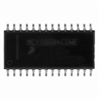
Manufacturer Part Number
MC908GR4CDWE
Description
IC MCU 4K FLASH 8MHZ 28-SOIC
Manufacturer
Freescale Semiconductor
Series
HC08r
Specifications of MC908GR4CDWE
Core Processor
HC08
Core Size
8-Bit
Speed
8MHz
Connectivity
SCI, SPI
Peripherals
LVD, POR, PWM
Number Of I /o
17
Program Memory Size
4KB (4K x 8)
Program Memory Type
FLASH
Ram Size
384 x 8
Voltage - Supply (vcc/vdd)
2.7 V ~ 5.5 V
Data Converters
A/D 6x8b
Oscillator Type
Internal
Operating Temperature
-40°C ~ 85°C
Package / Case
28-SOIC (7.5mm Width)
Controller Family/series
HC08
No. Of I/o's
21
Ram Memory Size
384Byte
Cpu Speed
8MHz
No. Of Timers
1
Embedded Interface Type
I2C, SCI, SPI
Rohs Compliant
Yes
Processor Series
HC08GR
Core
HC08
Data Bus Width
8 bit
Data Ram Size
384 B
Interface Type
SCI, SPI
Maximum Clock Frequency
8.2 MHz
Number Of Programmable I/os
21
Number Of Timers
3
Maximum Operating Temperature
+ 85 C
Mounting Style
SMD/SMT
Development Tools By Supplier
FSICEBASE, DEMO908GZ60E, M68CBL05CE, M68EML08GPGTE
Minimum Operating Temperature
- 40 C
On-chip Adc
8 bit, 6 Channel
Lead Free Status / RoHS Status
Lead free / RoHS Compliant
Eeprom Size
-
Lead Free Status / Rohs Status
Details


Flash Memory
11.7 FLASH Program/Read Operation
Technical Data
162
Programming of the FLASH memory is done on a row basis. A row
consists of 32 consecutive bytes starting from addresses $XX00,
$XX20, $XX40, $XX60, $XX80, $XXA0, $XXC0, and $XXE0. Use this
step-by-step procedure to program a row of FLASH memory
2
* The time between each FLASH address change, or the time between the last FLASH address
programmed to clearing PGM bit, must not exceed the maximum programming time, t
This program sequence is repeated throughout the memory until all data
is programmed.
10. Clear the PGM bit.*
11. Wait for a time, t
12. Clear the HVEN bit.
13. After time, t
is a flowchart representation):
1. Set the PGM bit. This configures the memory for program
2. Read from the FLASH block protect register.
3. Write any data to any FLASH address within the row address
4. Wait for a time, t
5. Set the HVEN bit.
6. Wait for a time, t
7. Write data to the FLASH address to be programmed.*
8. Wait for a time, t
9. Repeat step 7 and 8 until all the bytes within the row are
Freescale Semiconductor, Inc.
For More Information On This Product,
operation and enables the latching of address and data for
programming.
range desired.
programmed.
mode again.
Go to: www.freescale.com
rcv
Flash Memory
(min. 1 s), the memory can be accessed in read
nvs
pgs
PROG
nvh
(min. 10 s).
(min. 5 s).
(min. 5 s).
(min. 30 s).
MC68HC908GR8 — Rev 4.0
(Figure 11-
MOTOROLA
PROG
max.
Related parts for MC908GR4CDWE
Image
Part Number
Description
Manufacturer
Datasheet
Request
R

Part Number:
Description:
Manufacturer:
Freescale Semiconductor, Inc
Datasheet:
Part Number:
Description:
Manufacturer:
Freescale Semiconductor, Inc
Datasheet:
Part Number:
Description:
Manufacturer:
Freescale Semiconductor, Inc
Datasheet:
Part Number:
Description:
Manufacturer:
Freescale Semiconductor, Inc
Datasheet:
Part Number:
Description:
Manufacturer:
Freescale Semiconductor, Inc
Datasheet:
Part Number:
Description:
Manufacturer:
Freescale Semiconductor, Inc
Datasheet:
Part Number:
Description:
Manufacturer:
Freescale Semiconductor, Inc
Datasheet:
Part Number:
Description:
Manufacturer:
Freescale Semiconductor, Inc
Datasheet:
Part Number:
Description:
Manufacturer:
Freescale Semiconductor, Inc
Datasheet:
Part Number:
Description:
Manufacturer:
Freescale Semiconductor, Inc
Datasheet:
Part Number:
Description:
Manufacturer:
Freescale Semiconductor, Inc
Datasheet:
Part Number:
Description:
Manufacturer:
Freescale Semiconductor, Inc
Datasheet:
Part Number:
Description:
Manufacturer:
Freescale Semiconductor, Inc
Datasheet:
Part Number:
Description:
Manufacturer:
Freescale Semiconductor, Inc
Datasheet:
Part Number:
Description:
Manufacturer:
Freescale Semiconductor, Inc
Datasheet: