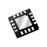
MC9S08QG84CFFER Freescale Semiconductor, MC9S08QG84CFFER Datasheet - Page 205

MC9S08QG84CFFER
Manufacturer Part Number
MC9S08QG84CFFER
Description
IC MCU 8BIT 8K FLASH 16-QFN
Manufacturer
Freescale Semiconductor
Series
HCS08r
Datasheet
1.MC9S08QG8CDTER.pdf
(314 pages)
Specifications of MC9S08QG84CFFER
Core Processor
HCS08
Core Size
8-Bit
Speed
20MHz
Connectivity
I²C, SCI, SPI
Peripherals
LVD, POR, PWM, WDT
Number Of I /o
12
Program Memory Size
8KB (8K x 8)
Program Memory Type
FLASH
Ram Size
512 x 8
Voltage - Supply (vcc/vdd)
1.8 V ~ 3.6 V
Data Converters
A/D 8x10b
Oscillator Type
Internal
Operating Temperature
-40°C ~ 85°C
Package / Case
16-QFN
Data Bus Width
8 bit
Maximum Clock Frequency
20 MHz
Data Ram Size
512 B
On-chip Adc
Yes
Number Of Programmable I/os
12
Number Of Timers
1
Mounting Style
SMD/SMT
Height
1 mm
Interface Type
I2C, SCI, SPI
Length
5 mm
Maximum Operating Temperature
+ 85 C
Minimum Operating Temperature
- 40 C
Supply Voltage (max)
3.6 V
Supply Voltage (min)
1.8 V
Width
5 mm
For Use With
DEMO9S08QG8E - BOARD DEMO FOR MC9S08QG8
Lead Free Status / RoHS Status
Lead free / RoHS Compliant
Eeprom Size
-
Lead Free Status / Rohs Status
Details
- Current page: 205 of 314
- Download datasheet (6Mb)
1
14.2.7
This register is actually two separate registers. Reads return the contents of the read-only receive data
buffer and writes go to the write-only transmit data buffer. Reads and writes of this register are also
involved in the automatic flag clearing mechanisms for the SCI status flags.
Freescale Semiconductor
Setting TXINV inverts the TxD output for all cases: data bits, start and stop bits, break, and idle.
Reset
TXINV
TXDIR
Field
ORIE
NEIE
FEIE
PEIE
5
4
3
2
1
0
W
R
1
SCI Data Register (SCID)
TxD Pin Direction in Single-Wire Mode — When the SCI is configured for single-wire half-duplex operation
(LOOPS = RSRC = 1), this bit determines the direction of data at the TxD pin.
0 TxD pin is an input in single-wire mode.
1 TxD pin is an output in single-wire mode.
Transmit Data Inversion — Setting this bit reverses the polarity of the transmitted data output.
0 Transmit data not inverted
1 Transmit data inverted
Overrun Interrupt Enable — This bit enables the overrun flag (OR) to generate hardware interrupt requests.
0 OR interrupts disabled (use polling).
1 Hardware interrupt requested when OR = 1.
Noise Error Interrupt Enable — This bit enables the noise flag (NF) to generate hardware interrupt requests.
0 NF interrupts disabled (use polling).
1 Hardware interrupt requested when NF = 1.
Framing Error Interrupt Enable — This bit enables the framing error flag (FE) to generate hardware interrupt
requests.
0 FE interrupts disabled (use polling).
1 Hardware interrupt requested when FE = 1.
Parity Error Interrupt Enable — This bit enables the parity error flag (PF) to generate hardware interrupt
requests.
0 PF interrupts disabled (use polling).
1 Hardware interrupt requested when PF = 1.
R7
T7
0
7
Table 14-7. SCIC3 Register Field Descriptions (continued)
R6
T6
0
6
MC9S08QG8 and MC9S08QG4 Data Sheet, Rev. 5
Figure 14-12. SCI Data Register (SCID)
R5
T5
0
5
R4
T4
0
4
Description
R3
T3
3
0
Serial Communications Interface (S08SCIV3)
R2
T2
0
2
R1
T1
0
1
R0
T0
0
0
203
Related parts for MC9S08QG84CFFER
Image
Part Number
Description
Manufacturer
Datasheet
Request
R
Part Number:
Description:
Hcs08 Microcontrollers
Manufacturer:
Freescale Semiconductor, Inc
Datasheet:
Part Number:
Description:
Manufacturer:
Freescale Semiconductor, Inc
Datasheet:
Part Number:
Description:
Manufacturer:
Freescale Semiconductor, Inc
Datasheet:
Part Number:
Description:
Manufacturer:
Freescale Semiconductor, Inc
Datasheet:
Part Number:
Description:
Manufacturer:
Freescale Semiconductor, Inc
Datasheet:
Part Number:
Description:
Manufacturer:
Freescale Semiconductor, Inc
Datasheet:
Part Number:
Description:
Manufacturer:
Freescale Semiconductor, Inc
Datasheet:
Part Number:
Description:
Manufacturer:
Freescale Semiconductor, Inc
Datasheet:
Part Number:
Description:
Manufacturer:
Freescale Semiconductor, Inc
Datasheet:
Part Number:
Description:
Manufacturer:
Freescale Semiconductor, Inc
Datasheet:
Part Number:
Description:
Manufacturer:
Freescale Semiconductor, Inc
Datasheet:
Part Number:
Description:
Manufacturer:
Freescale Semiconductor, Inc
Datasheet:
Part Number:
Description:
Manufacturer:
Freescale Semiconductor, Inc
Datasheet:
Part Number:
Description:
Manufacturer:
Freescale Semiconductor, Inc
Datasheet:
Part Number:
Description:
Manufacturer:
Freescale Semiconductor, Inc
Datasheet:


