ST72F561R9TA STMicroelectronics, ST72F561R9TA Datasheet - Page 252
ST72F561R9TA
Manufacturer Part Number
ST72F561R9TA
Description
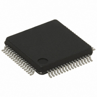
IC MCU 8BIT 60K FLASH 64-LQFP
Manufacturer
STMicroelectronics
Series
ST7r
Datasheet
1.ST72F561K6T6.pdf
(265 pages)
Specifications of ST72F561R9TA
Core Processor
ST7
Core Size
8-Bit
Speed
8MHz
Connectivity
CAN, LINSCI, SPI
Peripherals
LVD, POR, PWM, WDT
Number Of I /o
48
Program Memory Size
60KB (60K x 8)
Program Memory Type
FLASH
Ram Size
2K x 8
Voltage - Supply (vcc/vdd)
3.8 V ~ 5.5 V
Data Converters
A/D 16x10b
Oscillator Type
External
Operating Temperature
-40°C ~ 85°C
Package / Case
64-LQFP
For Use With
497-8374 - BOARD DEVELOPMENT FOR ST72F561
Lead Free Status / RoHS Status
Lead free / RoHS Compliant
Eeprom Size
-
Available stocks
Company
Part Number
Manufacturer
Quantity
Price
Company:

Part Number:
ST72F561R9TA
Manufacturer:
STMicroelectronics
Quantity:
10 000
Company:
Part Number:
ST72F561R9TATR
Manufacturer:
STMicroelectronics
Quantity:
10 000


ST72561
14 DEVICE CONFIGURATION AND ORDERING INFORMATION
Each device is available for production in user pro-
grammable versions (FLASH) as well as in factory
coded versions (ROM/FASTROM).
ST72561 devices are ROM versions. ST72P561
devices are Factory Advanced Service Technique
ROM (FASTROM) versions: They are factory-pro-
grammed HDFlash devices.
ST72F561 FLASH devices are shipped to custom-
ers with a default content (FFh), while ROM facto-
ry coded parts contain the code supplied by the
customer. This implies that FLASH devices have
to be configured by the customer using the Option
Bytes while the ROM devices are factory-config-
ured.
14.1 FLASH OPTION BYTES
The option bytes allows the hardware configura-
tion of the microcontroller to be selected. They
have no address in the memory map and can be
accessed only in programming mode (for example
using a standard ST7 programming tool). The de-
fault content of the FLASH is fixed to FFh. To pro-
gram directly the FLASH devices using ICP,
FLASH devices are shipped to customers with a
reserved internal clock source enabled. In masked
ROM devices, the option bytes are fixed in hard-
ware by the ROM code (see option list).
OPTION BYTE 0
OPT7 = WDGHALT Watchdog reset on HALT
This option bit determines if a RESET is generated
when entering HALT mode while the Watchdog is
(*): Option bit values programmed by ST
252/265
fault(*)
De-
7
1
WDG
1
STATIC OPTION BYTE 0
1
LVD
1
1
1
1
PKG
0
1
1
0
active.
0: No Reset generation when entering Halt mode
1: Reset generation when entering Halt mode
OPT6 = WDGSW Hardware or software watchdog
This option bit selects the watchdog type.
0: Hardware (watchdog always enabled)
1: Software (watchdog to be enabled by software)
OPT5 = Reserved, must be kept at default value.
OPT4 = LVD Voltage detection
This option bit enables the voltage detection block
(LVD).
OPT3 = PLL OFF PLL activation
This option bit activates the PLL which allows mul-
tiplication by two of the main input clock frequency.
The PLL is guaranteed only with an input frequen-
cy between 2 and 4 MHz.
0: PLL x2 enabled
1: PLL x2 disabled
Caution: The PLL can be enabled only if the “OSC
RANGE” (OPT11:10) bits are configured to “MP -
2~4 MHz”. Otherwise, the device functionality is
not guaranteed.
AFI_MAP
1
1
7
Selected Low Voltage Detector
0
1
STATIC OPTION BYTE 1
OSCTYPE OSCRANGE
1
1
LVD Off
LVD On
0
0
1
1
0
1
1
VD
1
0
0
1
Related parts for ST72F561R9TA
Image
Part Number
Description
Manufacturer
Datasheet
Request
R

Part Number:
Description:
STMicroelectronics [RIPPLE-CARRY BINARY COUNTER/DIVIDERS]
Manufacturer:
STMicroelectronics
Datasheet:
Part Number:
Description:
STMicroelectronics [LIQUID-CRYSTAL DISPLAY DRIVERS]
Manufacturer:
STMicroelectronics
Datasheet:

Part Number:
Description:
BOARD EVAL FOR MEMS SENSORS
Manufacturer:
STMicroelectronics
Datasheet:
Part Number:
Description:
NPN TRANSISTOR POWER MODULE
Manufacturer:
STMicroelectronics
Datasheet:
Part Number:
Description:
TURBOSWITCH ULTRA-FAST HIGH VOLTAGE DIODE
Manufacturer:
STMicroelectronics
Datasheet:
Part Number:
Description:
Manufacturer:
STMicroelectronics
Datasheet:
Part Number:
Description:
DIODE / SCR MODULE
Manufacturer:
STMicroelectronics
Datasheet:
Part Number:
Description:
DIODE / SCR MODULE
Manufacturer:
STMicroelectronics
Datasheet:
Part Number:
Description:
Search -----> STE16N100
Manufacturer:
STMicroelectronics
Datasheet:
Part Number:
Description:
Search ---> STE53NA50
Manufacturer:
STMicroelectronics
Datasheet:
Part Number:
Description:
NPN Transistor Power Module
Manufacturer:
STMicroelectronics
Datasheet:
Part Number:
Description:
DIODE / SCR MODULE
Manufacturer:
STMicroelectronics
Datasheet: