ST72F561R9TA STMicroelectronics, ST72F561R9TA Datasheet - Page 166
ST72F561R9TA
Manufacturer Part Number
ST72F561R9TA
Description
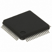
IC MCU 8BIT 60K FLASH 64-LQFP
Manufacturer
STMicroelectronics
Series
ST7r
Datasheet
1.ST72F561K6T6.pdf
(265 pages)
Specifications of ST72F561R9TA
Core Processor
ST7
Core Size
8-Bit
Speed
8MHz
Connectivity
CAN, LINSCI, SPI
Peripherals
LVD, POR, PWM, WDT
Number Of I /o
48
Program Memory Size
60KB (60K x 8)
Program Memory Type
FLASH
Ram Size
2K x 8
Voltage - Supply (vcc/vdd)
3.8 V ~ 5.5 V
Data Converters
A/D 16x10b
Oscillator Type
External
Operating Temperature
-40°C ~ 85°C
Package / Case
64-LQFP
For Use With
497-8374 - BOARD DEVELOPMENT FOR ST72F561
Lead Free Status / RoHS Status
Lead free / RoHS Compliant
Eeprom Size
-
Available stocks
Company
Part Number
Manufacturer
Quantity
Price
Company:

Part Number:
ST72F561R9TA
Manufacturer:
STMicroelectronics
Quantity:
10 000
Company:
Part Number:
ST72F561R9TATR
Manufacturer:
STMicroelectronics
Quantity:
10 000


ST72561
LINSCI™ SERIAL COMMUNICATION INTERFACE (LIN Master Only) (Cont’d)
CONTROL REGISTER 3 (SCICR3)
Read/Write
Reset Value: 0000 0000 (00h)
Bit 7 = Reserved, must be kept cleared.
Bit 6 = LINE LIN Mode Enable.
This bit is set and cleared by software.
0: LIN Mode disabled
1: LIN Master mode enabled
The LIN Master mode enables the capability to
send LIN Synch Breaks (13 low bits) using the
SBK bit in the SCICR2 register
.In transmission, the LIN Synch Break low phase
duration is shown as below:
Bits 5:4 = Reserved, forced by hardware to 0.
These bits are not used.
Bit 3 = CLKEN Clock Enable.
This bit allows the user to enable the SCLK pin.
0: SLK pin disabled
1: SLK pin enabled
Bit 2 = CPOL Clock Polarity.
This bit allows the user to select the polarity of the
clock output on the SCLK pin. It works in conjunc-
tion with the CPHA bit to produce the desired
clock/data relationship (see
93).
166/265
7
-
LINE
0
1
LINE
M
0
1
0
1
-
-
during a LIN Synch Break
Number of low bits sent
CLKEN CPOL CPHA
Figure 92
10
11
13
14
and
Figure
LBCL
0
0: Steady low value on SCLK pin outside transmis-
1: Steady high value on SCLK pin outside trans-
Bit 1 = CPHA Clock Phase.
This bit allows the user to select the phase of the
clock output on the SCLK pin. It works in conjunc-
tion with the CPOL bit to produce the desired
clock/data relationship (see
93)
0: SCLK clock line activated in middle of data bit.
1: SCLK clock line activated at beginning of data
Bit 0 = LBCL Last bit clock pulse.
This bit allows the user to select whether the clock
pulse associated with the last data bit transmitted
(MSB) has to be output on the SCLK pin.
0: The clock pulse of the last data bit is not output
1: The clock pulse of the last data bit is output to
Note: The last bit is the 8th or 9th data bit transmit-
ted depending on the 8 or 9 bit format selected by
the M bit in the SCICR1 register.
Table 26. SCI clock on SCLK pin
Note: These 3 bits (CPOL, CPHA, LBCL) should
not be written while the transmitter is enabled.
sion window.
mission window.
bit.
to the SCLK pin.
the SCLK pin.
format
Data
8 bit
9 bit
M bit
0
1
LBCL bit
1
0
0
1
Figure 92
Number of clock
pulses on SCLK
and
8
7
8
9
Figure
Related parts for ST72F561R9TA
Image
Part Number
Description
Manufacturer
Datasheet
Request
R

Part Number:
Description:
STMicroelectronics [RIPPLE-CARRY BINARY COUNTER/DIVIDERS]
Manufacturer:
STMicroelectronics
Datasheet:
Part Number:
Description:
STMicroelectronics [LIQUID-CRYSTAL DISPLAY DRIVERS]
Manufacturer:
STMicroelectronics
Datasheet:

Part Number:
Description:
BOARD EVAL FOR MEMS SENSORS
Manufacturer:
STMicroelectronics
Datasheet:
Part Number:
Description:
NPN TRANSISTOR POWER MODULE
Manufacturer:
STMicroelectronics
Datasheet:
Part Number:
Description:
TURBOSWITCH ULTRA-FAST HIGH VOLTAGE DIODE
Manufacturer:
STMicroelectronics
Datasheet:
Part Number:
Description:
Manufacturer:
STMicroelectronics
Datasheet:
Part Number:
Description:
DIODE / SCR MODULE
Manufacturer:
STMicroelectronics
Datasheet:
Part Number:
Description:
DIODE / SCR MODULE
Manufacturer:
STMicroelectronics
Datasheet:
Part Number:
Description:
Search -----> STE16N100
Manufacturer:
STMicroelectronics
Datasheet:
Part Number:
Description:
Search ---> STE53NA50
Manufacturer:
STMicroelectronics
Datasheet:
Part Number:
Description:
NPN Transistor Power Module
Manufacturer:
STMicroelectronics
Datasheet:
Part Number:
Description:
DIODE / SCR MODULE
Manufacturer:
STMicroelectronics
Datasheet: