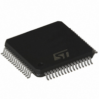
ST72F321AR9TA STMicroelectronics, ST72F321AR9TA Datasheet - Page 90

ST72F321AR9TA
Manufacturer Part Number
ST72F321AR9TA
Description
IC MCU 8BIT 60KB FLASH 64-TQFP
Manufacturer
STMicroelectronics
Series
ST7r
Datasheet
1.ST72F321AR7T6.pdf
(193 pages)
Specifications of ST72F321AR9TA
Core Processor
ST7
Core Size
8-Bit
Speed
8MHz
Connectivity
I²C, SCI, SPI
Peripherals
LVD, POR, PWM, WDT
Number Of I /o
48
Program Memory Size
60KB (60K x 8)
Program Memory Type
FLASH
Ram Size
2K x 8
Voltage - Supply (vcc/vdd)
3.8 V ~ 5.5 V
Data Converters
A/D 16x10b
Oscillator Type
Internal
Operating Temperature
-40°C ~ 85°C
Package / Case
64-TQFP, 64-VQFP
Lead Free Status / RoHS Status
Lead free / RoHS Compliant
Eeprom Size
-
Available stocks
Company
Part Number
Manufacturer
Quantity
Price
Company:
Part Number:
ST72F321AR9TA
Manufacturer:
ST
Quantity:
215
Company:
Part Number:
ST72F321AR9TA
Manufacturer:
STMicroelectronics
Quantity:
10 000
Part Number:
ST72F321AR9TA
Manufacturer:
ST
Quantity:
20 000
Company:
Part Number:
ST72F321AR9TAE
Manufacturer:
STMicroelectronics
Quantity:
10 000
Company:
Part Number:
ST72F321AR9TATR
Manufacturer:
STMicroelectronics
Quantity:
10 000
ST72321Rx ST72321ARx ST72321Jx
SERIAL PERIPHERAL INTERFACE (Cont’d)
10.5.3.2 Slave Select Management
As an alternative to using the SS pin to control the
Slave Select signal, the application can choose to
manage the Slave Select signal by software. This
is configured by the SSM bit in the SPICSR regis-
ter (see
In software management, the external SS pin is
free for other application uses and the internal SS
signal level is driven by writing to the SSI bit in the
SPICSR register.
In Master mode:
Figure 55. Generic SS Timing Diagram
Figure 56. Hardware/Software Slave Select Management
90/193
– SS internal must be held high continuously
MOSI/MISO
(if CPHA=0)
(if CPHA=1)
Figure
Master SS
Slave SS
Slave SS
56)
SS external pin
SSI bit
Byte 1
SSM bit
1
0
In Slave Mode:
There are two cases depending on the data/clock
timing relationship (see
If CPHA=1 (data latched on 2nd clock edge):
If CPHA=0 (data latched on 1st clock edge):
SS internal
Byte 2
– SS internal must be held low during the entire
– SS internal must be held low during byte
transmission. This implies that in single slave
applications the SS pin either can be tied to
V
ing the SS function by software (SSM= 1 and
SSI=0 in the in the SPICSR register)
transmission and pulled high between each
byte to allow the slave to write to the shift reg-
ister. If SS is not pulled high, a Write Collision
error will occur when the slave writes to the
shift register (see
SS
, or made free for standard I/O by manag-
Byte 3
Section
Figure
10.5.5.3).
55):


