ST7FLITE39F2B6 STMicroelectronics, ST7FLITE39F2B6 Datasheet - Page 23

ST7FLITE39F2B6
Manufacturer Part Number
ST7FLITE39F2B6
Description
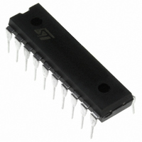
IC MCU 8BIT 8K FLASH 20DIP
Manufacturer
STMicroelectronics
Series
ST7r
Datasheet
1.ST7FLITE35F2M6TR.pdf
(173 pages)
Specifications of ST7FLITE39F2B6
Core Processor
ST7
Core Size
8-Bit
Speed
16MHz
Connectivity
LINSCI, SPI
Peripherals
LVD, POR, PWM, WDT
Number Of I /o
15
Program Memory Size
8KB (8K x 8)
Program Memory Type
FLASH
Eeprom Size
256 x 8
Ram Size
384 x 8
Voltage - Supply (vcc/vdd)
2.7 V ~ 5.5 V
Data Converters
A/D 7x10b
Oscillator Type
Internal
Operating Temperature
-40°C ~ 85°C
Package / Case
20-DIP (0.300", 7.62mm)
Processor Series
ST7FLITE3x
Core
ST7
Data Bus Width
8 bit
Data Ram Size
384 B
Interface Type
LINSCI, SPI
Maximum Clock Frequency
8 MHz
Number Of Programmable I/os
15
Number Of Timers
4
Maximum Operating Temperature
+ 85 C
Mounting Style
Through Hole
Development Tools By Supplier
ST7FLITE-SK/RAIS, ST7MDT10-DVP3, ST7MDT10-EMU3, STX-RLINK
Minimum Operating Temperature
- 40 C
On-chip Adc
10 bit, 7 Channel
For Use With
497-8406 - BOARD STF20NM50FD/STF7LITE39BF2497-8403 - BOARD DEMO STCC08 AC SW DETECTOR497-6398 - BOARD EVAL ST7FLITE39/STM1403497-5858 - EVAL BOARD PLAYBACK ST7FLITE497-5514 - EVAL BOARD THERMO CONTROL REFRIG497-5049 - KIT STARTER RAISONANCE ST7FLITE497-5046 - KIT TOOL FOR ST7/UPSD/STR7 MCU
Lead Free Status / RoHS Status
Lead free / RoHS Compliant
Other names
497-5634-5
Available stocks
Company
Part Number
Manufacturer
Quantity
Price
Company:
Part Number:
ST7FLITE39F2B6
Manufacturer:
STMicroelectronics
Quantity:
14
7 SUPPLY, RESET AND CLOCK MANAGEMENT
The device includes a range of utility features for
securing the application in critical situations (for
example in case of a power brown-out), and re-
ducing the number of external components.
Main features
■
■
■
7.1 INTERNAL RC OSCILLATOR ADJUSTMENT
The device contains an internal RC oscillator with
an accuracy of 1% for a given device, temperature
and voltage range (4.5V-5.5V). It must be calibrat-
ed to obtain the frequency required in the applica-
tion. This is done by software writing a 8-bit cali-
bration value in the RCCR (RC Control Register)
and in the bits [6:5] in the SICSR (SI Control Sta-
tus Register).
Whenever the microcontroller is reset, the RCCR
returns to its default value (FFh), i.e. each time the
device is reset, the calibration value must be load-
ed in the RCCR. Predefined calibration values are
stored in EEPROM for 3V and 5V V
ages at 25°C, as shown in the following table.
1. DEE0h, DEE1h, DEE2h and DEE3h addresses
are located in a reserved area of non-volatile
memory. They are read-only bytes for the applica-
RCCRH0
RCCRL0
RCCRH1
RCCRL1
– 1 MHz internal RC oscillator (enabled by op-
– 1 to 16 MHz or 32kHz External crystal/ceramic
– External Clock Input (enabled by option byte)
– PLL for multiplying the frequency by 8 or 4
– Main supply Low voltage detection (LVD) with
– Auxiliary Voltage detector (AVD) with interrupt
Clock Management
Reset Sequence Manager (RSM)
System Integrity Management (SI)
RCCR
tion byte, available on ST7LITE35 and
ST7LITE39 devices only)
resonator (selected by option byte)
(enabled by option byte)
reset generation (enabled by option byte)
capability for monitoring the main supply (en-
abled by option byte)
V
T
f
V
T
f
RC
RC
A
A
DD
DD
Conditions
=25°C
=25°C
=1MHz
=1MHz
=5V
=3.3V
DEE0h
DEE1h
DEE2h
DEE3h
Addresses
ST7LITE3
DD
1)
1)
1)
1)
(CR[9:2] bits)
(CR[1:0] bits)
(CR[9:2] bits)
(CR[1:0] bits)
supply volt-
tion code. This area cannot be erased or pro-
grammed by any ICC operation.
For compatibility reasons with the SICSR register,
CR[1:0] bits are stored in the 5th and 6th position
of DEE1 and DEE3 addresses.
Note:
– In 38-pulse ICC mode, the internal RC oscillator
– See “ELECTRICAL CHARACTERISTICS” on
– To improve clock stability and frequency accura-
– These bytes are systematically programmed by
– RCCR0 and RCCR1 calibration values will not
Caution: If the voltage or temperature conditions
change in the application, the frequency may need
to be recalibrated.
Refer to application note AN1324 for information
on how to calibrate the RC frequency using an ex-
ternal reference signal.
7.2 PHASE LOCKED LOOP
The PLL can be used to multiply a 1MHz frequen-
cy from the RC oscillator or the external clock by 4
or 8 to obtain f
bled and the multiplication factor of 4 or 8 is select-
ed by 2 option bits.
– The x4 PLL is intended for operation with V
– The x8 PLL is intended for operation with V
Refer to
tion.
If the PLL is disabled and the RC oscillator is ena-
bled, then f
is forced as a clock source, regardless of the se-
lection in the option byte. For ST7LITE30 devic-
es which do not support the internal RC
oscillator, the “option byte disabled” mode must
be used (35-pulse ICC mode entry, clock provid-
ed by the tool).
page 131. for more information on the frequency
and accuracy of the RC oscillator.
cy, it is recommended to place a decoupling ca-
pacitor, typically 100nF, between the V
V
ST, including on FASTROM devices. Conse-
quently, customers intending to use FASTROM
service must not use these bytes.
be erased if the read-out protection bit is reset af-
ter it has been set . See “Read out Protection” on
page 14.
the 2.7V to 3.3V range
the 3.3V to 5.5V range
SS
pins as close as possible to the ST7 device
Section 15.1
OSC =
OSC
1MHz.
of 4 or 8 MHz. The PLL is ena-
for the option byte descrip-
ST7LITE3xF2
DD
and
23/173
DD
DD
in
in
1


