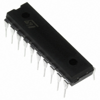
ST7FLITE39F2B6 STMicroelectronics, ST7FLITE39F2B6 Datasheet - Page 101

ST7FLITE39F2B6
Manufacturer Part Number
ST7FLITE39F2B6
Description
IC MCU 8BIT 8K FLASH 20DIP
Manufacturer
STMicroelectronics
Series
ST7r
Datasheet
1.ST7FLITE35F2M6TR.pdf
(173 pages)
Specifications of ST7FLITE39F2B6
Core Processor
ST7
Core Size
8-Bit
Speed
16MHz
Connectivity
LINSCI, SPI
Peripherals
LVD, POR, PWM, WDT
Number Of I /o
15
Program Memory Size
8KB (8K x 8)
Program Memory Type
FLASH
Eeprom Size
256 x 8
Ram Size
384 x 8
Voltage - Supply (vcc/vdd)
2.7 V ~ 5.5 V
Data Converters
A/D 7x10b
Oscillator Type
Internal
Operating Temperature
-40°C ~ 85°C
Package / Case
20-DIP (0.300", 7.62mm)
Processor Series
ST7FLITE3x
Core
ST7
Data Bus Width
8 bit
Data Ram Size
384 B
Interface Type
LINSCI, SPI
Maximum Clock Frequency
8 MHz
Number Of Programmable I/os
15
Number Of Timers
4
Maximum Operating Temperature
+ 85 C
Mounting Style
Through Hole
Development Tools By Supplier
ST7FLITE-SK/RAIS, ST7MDT10-DVP3, ST7MDT10-EMU3, STX-RLINK
Minimum Operating Temperature
- 40 C
On-chip Adc
10 bit, 7 Channel
For Use With
497-8406 - BOARD STF20NM50FD/STF7LITE39BF2497-8403 - BOARD DEMO STCC08 AC SW DETECTOR497-6398 - BOARD EVAL ST7FLITE39/STM1403497-5858 - EVAL BOARD PLAYBACK ST7FLITE497-5514 - EVAL BOARD THERMO CONTROL REFRIG497-5049 - KIT STARTER RAISONANCE ST7FLITE497-5046 - KIT TOOL FOR ST7/UPSD/STR7 MCU
Lead Free Status / RoHS Status
Lead free / RoHS Compliant
Other names
497-5634-5
Available stocks
Company
Part Number
Manufacturer
Quantity
Price
Company:
Part Number:
ST7FLITE39F2B6
Manufacturer:
STMicroelectronics
Quantity:
14
LINSCI™ SERIAL COMMUNICATION INTERFACE (SCI Mode) (cont’d)
CONTROL REGISTER 1 (SCICR1)
Read/Write
Reset Value: x000 0000 (x0h)
1)
Bit 7 = R8 Receive data bit 8
This bit is used to store the 9th bit of the received
word when M = 1.
Bit 6 = T8 Transmit data bit 8
This bit is used to store the 9th bit of the transmit-
ted word when M = 1.
Bit 5 = SCID Disabled for low power consumption
When this bit is set the SCI prescalers and outputs
are stopped and the end of the current byte trans-
fer in order to reduce power consumption.This bit
is set and cleared by software.
0: SCI enabled
1: SCI prescaler and outputs disabled
Bit 4 = M Word length
This bit determines the word length. It is set or
cleared by software.
0: 1 Start bit, 8 Data bits, 1 Stop bit
1: 1 Start bit, 9 Data bits, 1 Stop bit
Note: The M bit must not be modified during a data
transfer (both transmission and reception).
refer to the LIN mode register description.
This bit has a different function in LIN mode, please
R8
7
T8
SCID
M
WAKE PCE
1)
PS
PIE
0
Bit 3 = WAKE Wake-Up method
This bit determines the SCI Wake-Up method, it is
set or cleared by software.
0: Idle Line
1: Address Mark
Note: If the LINE bit is set, the WAKE bit is deacti-
vated and replaced by the LHDM bit.
Bit 2 = PCE Parity control enable
This bit is set and cleared by software. It selects
the hardware parity control (generation and detec-
tion for byte parity, detection only for LIN parity).
0: Parity control disabled
1: Parity control enabled
Bit 1 = PS Parity selection
This bit selects the odd or even parity when the
parity generation/detection is enabled (PCE bit
set). It is set and cleared by software. The parity
will be selected after the current byte.
0: Even parity
1: Odd parity
Bit 0 = PIE Parity interrupt enable
This bit enables the interrupt capability of the hard-
ware parity control when a parity error is detected
(PE bit set). The parity error involved can be a byte
parity error (if bit PCE is set and bit LPE is reset) or
a LIN parity error (if bit PCE is set and bit LPE is
set).
0: Parity error interrupt disabled
1: Parity error interrupt enabled
ST7LITE3xF2
101/173
1


