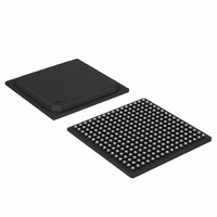
LH7A400N0G000B5;55 NXP Semiconductors, LH7A400N0G000B5;55 Datasheet - Page 54

LH7A400N0G000B5;55
Manufacturer Part Number
LH7A400N0G000B5;55
Description
IC ARM9 BLUESTREAK MCU 256BGA
Manufacturer
NXP Semiconductors
Series
BlueStreak ; LH7Ar
Datasheet
1.LH7A400N0F000B555.pdf
(65 pages)
Specifications of LH7A400N0G000B5;55
Core Size
16/32-Bit
Core Processor
ARM9
Speed
200MHz
Connectivity
EBI/EMI, IrDA, Microwire, MMC, SmartCard, SPI, SSI, SSP, UART/USART, USB
Peripherals
AC'97, DMA, LCD, POR, PWM, WDT
Number Of I /o
60
Program Memory Type
ROMless
Ram Size
80K x 8
Voltage - Supply (vcc/vdd)
1.71 V ~ 3.6 V
Oscillator Type
External
Operating Temperature
-40°C ~ 85°C
Package / Case
256-BGA
Controller Family/series
(ARM9)
No. Of I/o's
60
Ram Memory Size
80KB
Cpu Speed
200MHz
No. Of Timers
3
No. Of Pwm Channels
2
Digital Ic Case Style
BGA
Processor Series
LH7A4
Core
ARM9TDMI
Data Bus Width
32 bit
Mounting Style
SMD/SMT
3rd Party Development Tools
MDK-ARM, RL-ARM, ULINK2
Lead Free Status / RoHS Status
Lead free / RoHS Compliant
Eeprom Size
-
Program Memory Size
-
Data Converters
-
Lead Free Status / Rohs Status
Details
Other names
568-4334
935285038557
935285038557
LH7A400
CLOCK AND STATE CONTROLLER (CSC)
WAVEFORMS
coming out of Reset or Power On. Figure 43 shows exter-
nal reset timing, and Table 13 gives the timing parame-
ters. Figure 44 depicts signal timing following a Reset.
the 32.768 kHz oscillator is stable, and must be deas-
serted at least two 32.768 kHz clock periods before the
WAKEUP signal is asserted. Once the 14.7456 MHz
oscillator is stable, the PLLs require 250 µs to lock.
Boot), the Wakeup pin must not be asserted for 2 sec-
onds after assertion of nPOR to allow time for sampling
BATOK and nEXTPWR. The delay prevents a false
NOTE: *VDDC = VDDCmin
54
tOSC32
tOSC14
tURESET/tPWRFL nURESET/nPWRFL Pulse Width
Figure 42 shows the behavior of the LH7A400 when
At Power-On, nPOR must be held LOW at least until
On transition from Standby to Run (including a Cold
PARAMETER
32.768 kHz Oscillator Stabilization Time after Power On*
14.7456 MHz Oscillator Stabilization Time after Wake UP
T2
L8
(Horizontal Sync)
(Vertical Sync)
LCDHRLP
R2
Figure 41. AD-TFT and HR-TFT Vertical Timing Diagram
LCDSPS
(LCD Data)
LCDVD
LCDSPL
DESCRIPTION
Table 13. Reset AC Timing
Rev. 01 — 16 July 2007
NXP Semiconductors
1.5 µs - 4 µs
TIMING1:VSW
2x H-LINE
‘battery good’ indication caused by alkaline battery
recovery that can immediately follow a battery-low
switch off. The battery sampling takes place on the ris-
ing edge of the 1 Hz clock. This clock is derived from
the 32.768 kHz oscillator. The WAKEUP pin can be
pulsed, but at least one edge must follow the 2 second
delay to be recognized. For more information, see the
application note “Implementing Auto-Wakeup on the
LH7A4xx Series Devices” at www.nxp.com.
the NXP LH7A400 32.768 kHz external oscillator cir-
cuit. Figure 46 shows the same for the 14.7456 MHz
external oscillator circuit. In both figures, the NAND
gate represents the internal logic of the chip.
Figure 45 shows the recommended components for
MIN.
4
MAX.
550
4
32.768 kHz clock periods
32-Bit System-on-Chip
Preliminary data sheet
LH7A400-66
UNIT
ms
ms


