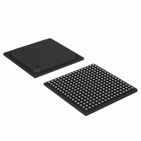
LH7A400N0G000B5;55 NXP Semiconductors, LH7A400N0G000B5;55 Datasheet - Page 33

LH7A400N0G000B5;55
Manufacturer Part Number
LH7A400N0G000B5;55
Description
IC ARM9 BLUESTREAK MCU 256BGA
Manufacturer
NXP Semiconductors
Series
BlueStreak ; LH7Ar
Datasheet
1.LH7A400N0F000B555.pdf
(65 pages)
Specifications of LH7A400N0G000B5;55
Core Size
16/32-Bit
Core Processor
ARM9
Speed
200MHz
Connectivity
EBI/EMI, IrDA, Microwire, MMC, SmartCard, SPI, SSI, SSP, UART/USART, USB
Peripherals
AC'97, DMA, LCD, POR, PWM, WDT
Number Of I /o
60
Program Memory Type
ROMless
Ram Size
80K x 8
Voltage - Supply (vcc/vdd)
1.71 V ~ 3.6 V
Oscillator Type
External
Operating Temperature
-40°C ~ 85°C
Package / Case
256-BGA
Controller Family/series
(ARM9)
No. Of I/o's
60
Ram Memory Size
80KB
Cpu Speed
200MHz
No. Of Timers
3
No. Of Pwm Channels
2
Digital Ic Case Style
BGA
Processor Series
LH7A4
Core
ARM9TDMI
Data Bus Width
32 bit
Mounting Style
SMD/SMT
3rd Party Development Tools
MDK-ARM, RL-ARM, ULINK2
Lead Free Status / RoHS Status
Lead free / RoHS Compliant
Eeprom Size
-
Program Memory Size
-
Data Converters
-
Lead Free Status / Rohs Status
Details
Other names
568-4334
935285038557
935285038557
32-Bit System-on-Chip
Power Supply Sequencing
energized before the 3.3 V supply. If this is not possi-
ble, the 1.8 V supply may not lag the 3.3 V supply by
more than 100 µs. If longer delay time is needed, it is
recommended that the voltage difference between the
two power supplies be within 1.5 V during power supply
ramp up.
should be applied to input pins only after the device is
powered-on as described above.
AC Specifications
tions after a reference clock signal. The illustration in
Figure 9 represents all cases of these sets of mea-
surement parameters.
• HCLK, internal System Bus clock (‘C’ in timing data)
• PCLK, Peripheral Bus clock
• SSPCLK, Synchronous Serial Port clock
• UARTCLK, UART Interface clock
• LCDDCLK, LCD Data clock from the
Preliminary data sheet
LCD Controller
NXP recommends that the 1.8 V power supply be
To avoid a potential latchup condition, voltage
All signals described in Table 12 relate to transi-
The reference clock signals in this design are:
REFERENCE
OUTPUT
SIGNAL (O)
INPUT
SIGNAL (I)
CLOCK
Figure 9. LH7A400 Signal Timing
tOVXXX
Rev. 01 — 16 July 2007
NXP Semiconductors
• ACBITCLK, AC97 clock
• SCLK, Synchronous Memory clock.
represents the amount of time for the output to become
valid from a valid address bus, or rising edge of the
peripheral clock. Maximum requirements for tOVXXX
are shown in Table 12.
amount of time the output will be held valid from the valid
address bus, or rising edge of the peripheral clock. Min-
imum requirements for tOHXXX are listed in Table 12.
of time the input signal must be valid before a valid
address bus, or rising edge of the peripheral clock
(except SSP and ACI). Maximum requirements for
tISXXX are shown in Table 12.
amount of time the output must be held valid from the
valid address bus, or rising edge of the peripheral clock
(except SSP and ACI). Minimum requirements are
shown in Table 12.
tISXXX tIHXXX
All signal transitions are measured at the 50 % point.
For outputs from the LH7A400, tOVXXX (e.g. tOVA)
The signal tOHXXX (e.g. tOHA) represents the
For Inputs, tISXXX (e.g. tISD) represents the amount
The signal tIHXXX (e.g. tIHD) represents the
tOHXXX
LH7A400
7A400-28
33


